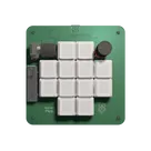
PCB Design for Cinema Camera Power Distribution
Thought for 2 sec
- Connected U2:RTN, R12:P2, C14:P2, R14:P2, R16:P2, R10:P2, U2:MODE to ^TPS_RTN
- Disconnected U2:RTN, R12:P2, C14:P2, R14:P2, R16:P2, R10:P2, U2:MODE
Thought for 1 sec
- Set C13's Capacitance to "22uF"
- Set C13's Voltage Rating to "10V"
- Set C13's Role Details to "AMS1117 output stability capacitor, >=22uF placed close to VOUT and SGND"
- Set C14's Capacitance to "22nF"
- Set C14's Role to "Timing"
- Set C14's Role Details to "TPS26600 dVdT capacitor from dVdT to RTN; 22nF gives controlled output ramp per TI example"
- Set R12's Resistance to "5.36kohms"
- Set R12's Tolerance to "1%"
- Set R12's Role Details to "TPS26600 ILIM resistor to RTN; 5.36k sets maximum supported ~2.23A overload limit"
- Set R13's Resistance to "715kohms"
- Set R13's Tolerance to "1%"
- Set R13's Role Details to "TPS26600 UVLO/OVP upper divider element for ~18V UVLO and ~30V OVP reference network"
- Set R14's Resistance to "20kohms"
- Set R14's Tolerance to "1%"
- Set R14's Role Details to "TPS26600 UVLO/OVP middle divider element feeding UVLO node"
- Set R15's Resistance to "30.1kohms"
- Set R15's Tolerance to "1%"
- Set R15's Role Details to "TPS26600 UVLO/OVP lower divider element feeding OVP node to RTN"
- Set R16's Resistance to "0ohms"
- Set R16's Role Details to "Placeholder/strap to tie OVP lower reference to TPS_RTN if using default/derived OVP scheme; verify against final divider top..."
Refine this doc
Ask about this doc
Project Specification: RED KOMODO-X Power IO Distribution
Goal
Design a 75×66mm 2-layer FR4 1.6mm PCB with 2oz copper on both layers for a professional RED KOMODO-X cinema camera power and IO distribution device. External panel connectors connect by soldered flying leads only; the PCB uses edge solder-pad terminals, not connector footprints.
Architecture
Diagram
Required Components
- LTC4412IS6 OR controller, TPS26600PWPR master switch, AMS1117-3.3 LDO
- AO3401A P-channel MOSFETs ×2, SI2302 tally MOSFET
- SMAJ18A ×2, SMAJ5.0A ×1, BAT54 ×1, BLM18AG601SH1D ×2
- 100uF 25V electrolytic bulk, 100nF 0402 ×10, 10uF 0402 ×4, 0402 resistors ×18, 0603 LEDs ×3
- Four M3 mounting holes 5mm inset from corners
- Edge solder-pad terminals for all external flying leads
Layout Requirements
- Board: 75×66mm rectangle, FR4, 1.6mm, 2-layer, 2oz copper both sides
- Top: components and signal traces
- Bottom: ground plane with power pours and via stitching on power nodes
- Power input components bottom edge
- ORing and TPS26600 lower center
- AMS1117 and signal/IO components upper half
- Edge solder pads grouped by function with pad labels
- Signal and power ground pours split and connected at a single star point near the lower-left main power input
Notes and Assumptions
- Since panel connectors are external, PCB external interfaces are implemented as solder pads with named nets.
- A library-compatible BLM18AG601 series ferrite bead is used for the requested Murata BLM18AG601SH1D function.
- The resettable 6A breaker is represented in the schematic as a labeled series element/terminal path for the aux rail unless an exact breaker footprint is added later.
- TPS26600 design note: the selected TPS26600PWPR is a 2.23A-max eFuse when RILIM is set to 5.36k. This is below a true 6A camera/aux distribution path, so the schematic uses the selected device but this current-rating mismatch must be reviewed before production if the main bus is expected to carry camera plus accessory current above roughly 2A.
- TPS26600 RTN note: RTN is kept as a separate support-component reference net for ILIM, dVdT, MODE, SHDN bias, and UVLO/OVP divider returns; it is not intentionally shorted to PGND so reverse-polarity behavior is not defeated.
- AMS1117 stability note: the 3.3V output capacitor is set to 22uF minimum per AMS1117 stability guidance and should be placed close to VOUT/SGND.
Goal
Architecture
Required Components
Layout Requirements
Notes and Assumptions