Project Overview and Analysis
1:49
Project
Here’s a concise technical overview of your “ESPRESSO32 Smart Scale AI Auto Layouted” project based on the schematic and nets in the project context.
Purpose and high-level architecture
- Purpose: A connected smart scale platform using an ESP32-C3 for control/communications, a precision 24-bit ADC for load cell measurements, and a power system that accepts 12 V input, generates 5 V and 3.3 V rails, and exposes USB and expansion headers. It showcases AI Auto Layout workflows and good rulesets/zones/fanout practices.
- Core rails:
- PP12V0: primary input.
- PP5V0: buck-regulated from 12 V; also feeds peripherals and the ADC.
- PP3V3: LDO-regulated from 5 V; powers the ESP32-C3 and digital logic.
- Key data paths:
- Load cell bridge to NAU7802 ADC → I2C to ESP32-C3.
- Optional SPI/SD signals broken out (J1 looks like a microSD connector).
- USB-C connector included (likely for power, comms, or mechanical demonstration).
Core components and interactions
- MCU and RF front-end
- IC1: main controller with Wi-Fi/BLE. Powered by PP3V3 and PP3V3_L domains with decoupling.
- RF matching/antenna path uses L1, L4, C6 and chip antenna Y2. The “LNA_IN” network and coupler path “LNA_IN_C”/“LNA_IN_L” indicate a tuned 2.4 GHz front-end to the on-board antenna.
- 40 MHz crystal network Y1 with loading caps C8 and C4 tied to XTAL_P/XTAL_N.
- Precision measurement front-end
- U1: 24-bit load-cell ADC with integrated PGA and reference.
- Load cell inputs: LOAD_CELL_A1_P/AI_N nets via series protection/RC components R2 and R4, and filtering C20. Reference and analog supplies decoupled (C11, C23, C3, C31 group).
- Interface to MCU: I2C (I2C_SDA, I2C_SCL) with pull-ups R1 and R5. DRDY interrupt to MCU via INT_ADC_DRDY.
- Power subsystem
- Connectors and expansion
- microSD/socket J1: SPI_CS/SCK/MOSI/MISO nets indicate SPI storage or external peripheral.
- Load-cell connector J3 ties to the filtered AIN_P/AIN_N and shield/ground.
- GPIO header J4 breaks out GPIO_SW1/SW2 and GND.
- Test pads MCU_TXD, MCU_RXD, MCU_BOOT.
- USB-C J2 present; D+/D- are on MCU pins USBC2.0_D_P/N for potential comms or demo; ESD/CC handling not shown in this slice, so likely power-only or simplified IO.
- Decoupling and filtering
- Extensive 1 uF and 10 uF caps on each rail cluster, plus local 0.1 uF at noise-sensitive nodes (e.g., C23 for ADC VBG).
- Series L/C filtering on PP3V3_L (L2 with downstream decouplers C12/C21/C13/C5/C18) to isolate RF/analog domains from core 3.3 V.
Design, implementation, and functionality
- Power-up sequence: 12 V → Buck to 5 V (PP5V0). Buck PG gates the LDO EN, enabling 3.3 V (PP3V3). The MCU and digital rails come up after 5 V is valid, reducing brownout risk.
- Measurement chain: Load cell differential signals enter via J3, pass through series resistors and RC filter to the NAU7802 VIN1P/N. The ADC’s DRDY pulses go to the ESP32 for synchronized reads over I2C.
- Communications and storage: ESP32 provides Wi‑Fi/BLE, optional SPI interface to J1 for data logging, and UART test pads for development. D+/D- nets on MCU suggest potential USB-CDC or debugging over USB-C (depends on firmware and CC wiring).
- RF: The front-end network provides impedance matching between the ESP32 LNA input and the 2.4 GHz chip antenna for robust wireless links.
- User I/O: Two GPIOs broken out to a 3-pin header for external switches or sensors.
Key technologies, dependencies, and design choices
- Dependencies:
- Firmware for ESP32-C3 (I2C driver for NAU7802, SPI/SD if used, Wi‑Fi/BLE stack).
- NAU7802 register config (gain, rate, filters, calibration).
- Design choices and trade-offs:
- 12 V input with synchronous buck to 5 V then LDO to 3.3 V: favors noise performance for the MCU/RF/ADC by isolating 3.3 V with an LDO and additional LC filtering. Trade-off: lower efficiency than a direct 12 V → 3.3 V buck.
- Tying LDO EN to buck PG: simple and robust sequencing; relies on correct PG thresholds of the buck.
- ESP32-C3 integrated RF with compact matching vs external PA/LNA: smaller, simpler, adequate for most IoT ranges; trade-off against maximum RF range.
- NAU7802 as an integrated high-resolution ADC: simplifies precision load cell interface vs discrete instrumentation amp + ADC; performance hinges on layout, shielding, and stable references.
- Extensive decoupling and LC segmentation on PP3V3_L: improves analog/RF stability; consumes area and BOM.
Potential challenges and performance considerations
- Analog integrity: Load cell signals are microvolt-level. PCB layout must maintain symmetry, short sensor leads, guard grounds, and minimize thermocouple errors at copper junctions. Ensure the shield pin on J3 is grounded appropriately and the sensor cable routing avoids RF fields.
- Grounding: Star/directed return for ADC analog ground vs high di/dt switching ground of the buck. Keep SW node (U3:SW, L3) compact and far from ADC inputs and RF.
- RF performance: Matching network and keep-out area around the antenna are critical. Ensure proper ground clearance and tuning room if enclosure detunes the antenna.
- USB-C correctness: If data is intended, ensure CC resistors/USB mux/ESD present; otherwise, clarify power-only to avoid host/device confusion.
- Thermal: At higher 12 V input currents, buck inductor and IC thermals matter; also LDO dissipation if 3.3 V rail current is high. Check headroom and dropout limits on NCP176.
- SD/SPI signal integrity: If long runs, consider series damping resistors and solid ground reference to the socket.
Real-world applications
- Smart kitchen scale, coffee scale (espresso), postal scale, or load monitoring node with wireless connectivity, logging to SD, and mobile app control.
- Teaching/demonstration platform for AI Auto Layout, ruleset creation, and mixed-signal/RF-power co-design.
Areas for improvement and future enhancements
- Power path:
- Consider a second buck to generate 3.3 V directly from 12 V for better efficiency, keeping an LDO only for ultra-quiet analog/RF islands.
- Add input protection: TVS on 12 V, reverse polarity/OVP, and EMI input filter (π filter).
- USB-C:
- Add CC resistors/PD controller for correct role detection; add ESD diodes on D+/D- and VBUS.
- If only for power, mark as 5 V power-only with proper CC config and omit D+/D- routing.
- ADC/analog:
- Add RC common-mode filter and optional RC at the reference pins, plus footprints for ferrites to isolate analog reference/supply.
- Provide Kelvin-connected ground and short, symmetric routes for VINP/N. Add guard rings if feasible.
- RF:
- Reserve tuning component footprints and ensure antenna keep-out and ground clearance follow vendor app notes. Consider an external u.FL option for chamber tuning.
- Firmware/debug:
- Expose JTAG (if needed) and a reset button. Keep BOOT/EN circuitry with proper pull-ups/pull-downs and debounced user buttons.
- DFM/EMC:
- Add test points on all rails, place PG/EN measurement pads, and include mounting/ground stitching vias near connectors for robustness.
- Scalability:
- Modularize sensors via a dedicated I2C/SPI expansion connector with power and IRQ.
- Power budget headroom for additional sensors or displays; consider 5 V peripherals on PP5V0 and translate where needed.
If you want, I can review ERC/DRC and power integrity in this project and suggest specific component value tweaks or placement/routing notes, or help plan targeted improvements.
Run ERC/DRC
ADC routing
Input protection
RF grounding
Power integrity
120 days
Ready.
PP5V0
R3
Resistance
10k Ω
C7
Capacitance
1u F
C13
Capacitance
1u F
C23
Capacitance
.1u F
PG_PP5V0
R1
Resistance
10k Ω
C18
Capacitance
1u F
USBC2.0_D_N
C20
Capacitance
1u F
SPI_MISO
I2C_SDA
H4
PP3V3
H1
C2
Manufacturer Part Number
OPT
PP3V3
SPI_SCK
USBC2.0_D_P
C10
Capacitance
1u F
I2C_SCL
PP3V3_SPI
C25
Capacitance
22u F
LOAD_CELL_A1_P
PP3V3
C15
Capacitance
1u F
Y1
R7
Resistance
100k Ω
L1
Inductance
2.2n H
R8
Resistance
953k Ω
SPI_SCK
PP5V0
LOAD_CELL_A1_P
H2
C5
Capacitance
1u F
INT_ADC_DRDY
R5
Resistance
10k Ω
PP3V3
LOAD_CELL_AI_N
C8
Capacitance
13p F
GPIO_SW1
C12
Capacitance
1u F
I2C_SDA
GPIO_SW2
C11
Capacitance
1u F
SPI_MISO
H3
C6
Capacitance
1.2p F
C24
Capacitance
1u F
PP12V0
SPI_MOSI
R6
Resistance
180k Ω
LOAD_CELL_AI_N
L2
Inductance
2.2n H
I2C_SCL
SPI_CS
C31
Capacitance
.1u F
VOS
PP3V3
PP3V3
SPI_CS
SPI_MOSI
C4
Capacitance
13p F
IC1
U2
C22
Capacitance
10u F
MCU_TXD
J1
C21
Capacitance
10u F
Y2
L4
C30
Capacitance
10u F
C1
Capacitance
10u F
MCU_RXD
L3
Inductance
2.2u H
MCU_BOOT
Reviews

- Wirelessly connects nets on schematic. Used to organize schematics and separate functional blocks. To wirelessly connect net portals, give them same designator. #portaljharwinbarrozo43.0M
- Wirelessly connects power nets on schematic. Identical to the net portal, but with a power symbol. Used to organize schematics and separate functional blocks. To wirelessly connect power net portals, give them the same designator. #portal #powerjharwinbarrozo11.4M
- A generic fixed resistor for rapid developing circuit topology. Save precious design time by seamlessly add more information to this part (value, footprint, etc.) as it becomes available. Standard resistor values: 1.0Ω 10Ω 100Ω 1.0kΩ 10kΩ 100kΩ 1.0MΩ 1.1Ω 11Ω 110Ω 1.1kΩ 11kΩ 110kΩ 1.1MΩ 1.2Ω 12Ω 120Ω 1.2kΩ 12kΩ 120kΩ 1.2MΩ 1.3Ω 13Ω 130Ω 1.3kΩ 13kΩ 130kΩ 1.3MΩ 1.5Ω 15Ω 150Ω 1.5kΩ 15kΩ 150kΩ 1.5MΩ 1.6Ω 16Ω 160Ω 1.6kΩ 16kΩ 160kΩ 1.6MΩ 1.8Ω 18Ω 180Ω 1.8KΩ 18kΩ 180kΩ 1.8MΩ 2.0Ω 20Ω 200Ω 2.0kΩ 20kΩ 200kΩ 2.0MΩ 2.2Ω 22Ω 220Ω 2.2kΩ 22kΩ 220kΩ 2.2MΩ 2.4Ω 24Ω 240Ω 2.4kΩ 24kΩ 240kΩ 2.4MΩ 2.7Ω 27Ω 270Ω 2.7kΩ 27kΩ 270kΩ 2.7MΩ 3.0Ω 30Ω 300Ω 3.0KΩ 30KΩ 300KΩ 3.0MΩ 3.3Ω 33Ω 330Ω 3.3kΩ 33kΩ 330kΩ 3.3MΩ 3.6Ω 36Ω 360Ω 3.6kΩ 36kΩ 360kΩ 3.6MΩ 3.9Ω 39Ω 390Ω 3.9kΩ 39kΩ 390kΩ 3.9MΩ 4.3Ω 43Ω 430Ω 4.3kΩ 43KΩ 430KΩ 4.3MΩ 4.7Ω 47Ω 470Ω 4.7kΩ 47kΩ 470kΩ 4.7MΩ 5.1Ω 51Ω 510Ω 5.1kΩ 51kΩ 510kΩ 5.1MΩ 5.6Ω 56Ω 560Ω 5.6kΩ 56kΩ 560kΩ 5.6MΩ 6.2Ω 62Ω 620Ω 6.2kΩ 62KΩ 620KΩ 6.2MΩ 6.8Ω 68Ω 680Ω 6.8kΩ 68kΩ 680kΩ 6.8MΩ 7.5Ω 75Ω 750Ω 7.5kΩ 75kΩ 750kΩ 7.5MΩ 8.2Ω 82Ω 820Ω 8.2kΩ 82kΩ 820kΩ 8.2MΩ 9.1Ω 91Ω 910Ω 9.1kΩ 91kΩ 910kΩ 9.1MΩ #generics #CommonPartsLibraryjharwinbarrozo1.5M
- A generic fixed capacitor ideal for rapid circuit topology development. You can choose between polarized and non-polarized types, its symbol and the footprint will automatically adapt based on your selection. Supported options include standard SMD sizes for ceramic capacitors (e.g., 0402, 0603, 0805), SMD sizes for aluminum electrolytic capacitors, and through-hole footprints for polarized capacitors. Save precious design time by seamlessly add more information to this part (value, footprint, etc.) as it becomes available. Standard capacitor values: 1.0pF 10pF 100pF 1000pF 0.01uF 0.1uF 1.0uF 10uF 100uF 1000uF 10,000uF 1.1pF 11pF 110pF 1100pF 1.2pF 12pF 120pF 1200pF 1.3pF 13pF 130pF 1300pF 1.5pF 15pF 150pF 1500pF 0.015uF 0.15uF 1.5uF 15uF 150uF 1500uF 1.6pF 16pF 160pF 1600pF 1.8pF 18pF 180pF 1800pF 2.0pF 20pF 200pF 2000pF 2.2pF 22pF 20pF 2200pF 0.022uF 0.22uF 2.2uF 22uF 220uF 2200uF 2.4pF 24pF 240pF 2400pF 2.7pF 27pF 270pF 2700pF 3.0pF 30pF 300pF 3000pF 3.3pF 33pF 330pF 3300pF 0.033uF 0.33uF 3.3uF 33uF 330uF 3300uF 3.6pF 36pF 360pF 3600pF 3.9pF 39pF 390pF 3900pF 4.3pF 43pF 430pF 4300pF 4.7pF 47pF 470pF 4700pF 0.047uF 0.47uF 4.7uF 47uF 470uF 4700uF 5.1pF 51pF 510pF 5100pF 5.6pF 56pF 560pF 5600pF 6.2pF 62pF 620pF 6200pF 6.8pF 68pF 680pF 6800pF 0.068uF 0.68uF 6.8uF 68uF 680uF 6800uF 7.5pF 75pF 750pF 7500pF 8.2pF 82pF 820pF 8200pF 9.1pF 91pF 910pF 9100pF #generics #CommonPartsLibraryjharwinbarrozo1.5M
- A generic fixed inductor for rapid developing circuit topology. *You can now change the footprint and 3D model at the top level anytime you want. This is the power of #genericsjharwinbarrozo15.5k
- An electrical connector acting as reusable interface to a conductor and creating a point where external circuits can be connected.Terminal
- 47 kOhms ±5% 0.125W, 1/8W Chip Resistor 0805 (2012 Metric) Automotive AEC-Q200 Thick Film #forLedBlinkjharwinbarrozo1.2M
- 10uF Capacitor Aluminum Polymer 20% 16V SMD 5x5.3mm #forLedBlink #commonpartslibrary #capacitor #aluminumpolymer #radialcanjharwinbarrozo1.2M
- Yellow 595nm LED Indication - Discrete 1.7V 1206 (3216 Metric) #forLedBlinkjharwinbarrozo1.1M


Learn how to use AI Auto Layout on this ESP32 Espresso Smart Scale! In one click you’ll see AI Auto Layout perform magic. Pay close attention to how we recommend creating rulesets, zones, and fanouts. By copying the setup in this example on your own project, you’ll have a fully routed board in no time!
Properties
Properties describe core aspects of the project.
Pricing & Availability
Distributor | Qty 1 |
|---|---|
Arrow | $3.76–$4.70 |
Digi-Key | $6.29–$10.05 |
LCSC | $6.75–$7.60 |
Mouser | $8.56 |
Verical | $1.70–$2.37 |
Assets
dxf
ESPRESSO32 Smart Scale Board Outline.dxf
ESPRESSO32 Smart Scale Board Outlinedxf
ESPRESSO32 Smart Scale Antenna Cutout.dxf
ESPRESSO32 Smart Scale Antenna Cutout
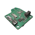
ESPRESSO32_Smart_Scale_3D_Thumnail.png
ESPRESSO32_Smart_Scale_3D_ThumnailThumbnailControls
Welcome 👋
Flux helps you build PCBs faster with an AI teammate!
Create your account to collaborate, stay updated, fork your own version, and get instant answers from our AI agent.