Schematic Design Analysis
1:50
Project
Below is a schematic-level analysis based solely on the provided design information:
1. Regulator & Feedback Network Connections
-
Issue: U3 (SY6280) Pin Misassignment
– Observation: The net labeled VIN shows that both the VIN and EN pins of U3 are tied together. For the SY6280 (pins: VOUT, GND, ISET, EN, VIN), the EN pin should be driven (typically via a pull‐up or by logic) rather than being hardwired with the input voltage.
– Recommendation: Separate U3’s EN from its VIN. Tie EN to the proper logic (or use a resistor divider/pull‑up if that is the intent) per the datasheet recommendation. -
Issue: Shared Divider Resistor (R3) Across Different Nets
– Observation: Resistor R3 has one terminal on net FB (used for U1’s feedback) and the other on net VIN (which also carries U3 VIN/EN). This forces an unexpected connection between two regulator sections that should be independent.
– Recommendation: Redefine the feedback divider so that each regulator (U1 and U3) has its own, isolated divider network. In particular, re‑assign R3’s connections so that the divider for U1’s FB is not shorted to U3’s power section. -
Issue: Conflicting Voltage Divider Formulas
– Observation: The text note “SETTING OUTPUT VOLTAGE” shows two formulas:- VOUT=VREF×(1+R9R6)
- VOUT=VREF×(1+(R1+R4)R6)
This suggests either a design revision or a leftover note from an earlier revision.
– Recommendation: Decide on one feedback network configuration. Remove or update the annotation to reflect the chosen resistor divider between the correct regulator output and its FB pin.
2. Power Distribution & Net Labeling
-
Issue: Duplicate and Ambiguous Net Labels
– Observation: Several portals use similar or duplicate names (for example, multiple “Ground” objects, “12_5V” vs. “12V_DIV” nets) and some nets appear in more than one context (e.g. “VIN” carries U3 VIN and also ties in divider elements for U1).
– Recommendation:- Ensure that each power rail (battery, solar, USB, regulated outputs) is clearly defined with a unique net name.
- Verify that regulator inputs, outputs, and feedback networks use separate nets unless intentional.
- Use consistent naming (for example, avoid “12_5V” and “12V_DIV” if they refer to the same rail or divider) so that the intended connectivity is unambiguous during layout and DRC checks.
-
Issue: Potential Overlap of Regulator Sections
– Observation: The sharing of net VIN between U3 (a SY6280 regulator) and the feedback divider of U1 (RT8059) suggests that their power paths might interfere.
– Recommendation: Completely separate the power and control nets for each converter so that no accidental bridging (for instance, tying U3’s EN/VIN with U1’s divider) occurs.
3. Decoupling Capacitors & Bypass Networks
- Issue: Decoupling Capacitor Placement Uncertainty
– Observation: Although several capacitors (e.g. C1, C2, C8, C9) are present on the schematic, their placement relative to the regulator ICs is not explicitly shown. Given the high switching frequency of devices like the MT3608 and likely for the RT8059, nearby bypass/external output capacitors are critical.
– Recommendation:- Confirm that each regulator has at least one decoupling capacitor placed as close as possible to its VIN, VOUT, and FB pins (if recommended), following datasheet recommendations.
- If not already done, move the decoupling capacitors (for example, C2 for U3’s VIN and C8 for the FB divider) to minimize parasitic inductance.
4. Current Limiting & LED Drive
- Issue: LED Current Limiting
– Observation: The schematic includes two LED components (D5 and D2) with forward voltages and current ratings given, but there is no series resistor explicitly associated with them. Directly connecting an LED to a power rail without a current‐limiting resistor can cause overcurrent damage.
– Recommendation:- Insert an appropriate current-limiting resistor in series with each LED. For example, for a red LED with a forward voltage around 2.0 V and a target current of 20 mA at a 5V supply, calculate the resistor as:
R=0.02A5V−2V=150Ω.
- Insert an appropriate current-limiting resistor in series with each LED. For example, for a red LED with a forward voltage around 2.0 V and a target current of 20 mA at a 5V supply, calculate the resistor as:
5. General Signal Integrity & Connectivity
-
Issue: Inconsistent Pin and Net Assignments
– Observation: Some components (for instance, the connections of U4 [CN3063] used for battery charging) show mixed signals across different nets (e.g., its FB and ISET nodes share nets with divider or other signals).
– Recommendation:- Recheck each IC’s pin assignment against its datasheet. For U4, verify that the pins for temperature, charge control (~DONE, ~CHARG) and feedback are routed to the appropriate nets.
- Ensure that signal nets, especially those that interface with control or feedback pins, are not inadvertently tied to power rails.
-
Issue: Layout Considerations Not Shown on Schematic
– Observation: While this analysis is schematic-level, note that good PCB practices (such as short, wide power traces, adequate spacing for high-frequency switching nodes, and proper ground plane continuity) are essential for minimizing EMI and other signal integrity issues.
– Recommendation:- During layout, verify that high-frequency switching nodes from converters like MT3608 and RT8059 are kept short with their decoupling components, and use proper trace width and via stitching to maintain a robust low‑impedance ground.
Summary of Corrections
| Issue | Location/Component(s) | Correction/Optimization |
|---|---|---|
| U3 EN tied to VIN | U3 (SY6280) EN and VIN pins | Separate these signals; drive EN via appropriate logic/control rather than directly tying to VIN. |
| Shared resistor R3 across FB and VIN | R3 between U1 feedback network and U3 VIN | Isolate the divider networks; assign separate resistor(s) for each regulator’s FB node. |
| Conflicting voltage divider note | “SETTING OUTPUT VOLTAGE” text note | Update the note to reflect a single, verified divider scheme for the chosen regulator. |
| Ambiguous and duplicate net labels | Multiple power nets (VIN, 12_5V, 12V_DIV, Ground, etc.) | Re‑label and segregate power/feedback nets to ensure clear and isolated paths. |
| Decoupling capacitor placement uncertainty | Across regulators (e.g. U1, U3, MT3608) | Verify placements in layout to be as close as possible to the respective IC pins. |
| Missing LED current limit resistors | LED components D5 and D2 | Insert series resistors (≈150 Ω for 5V operation with 2V forward drop at 20 mA). |
| Potential misconnection of U4 signals | U4 (CN3063) charge controller | Double-check each pin’s connection against its datasheet to ensure proper function. |
By addressing these specific areas, you will reduce the risk of electrical conflicts and improve both the performance and reliability of the power management board.
Fix U3 EN connection
Correct shared R3 issue
Clarify divider formula note
Improve net labeling
Ensure decoupling capacitor placement
388 days
Ready.
J1
VBAT
Reviews

- Wirelessly connects nets on schematic. Used to organize schematics and separate functional blocks. To wirelessly connect net portals, give them same designator. #portaljharwinbarrozo43.0M
- Wirelessly connects power nets on schematic. Identical to the net portal, but with a power symbol. Used to organize schematics and separate functional blocks. To wirelessly connect power net portals, give them the same designator. #portal #powerjharwinbarrozo11.4M
- A generic fixed resistor for rapid developing circuit topology. Save precious design time by seamlessly add more information to this part (value, footprint, etc.) as it becomes available. Standard resistor values: 1.0Ω 10Ω 100Ω 1.0kΩ 10kΩ 100kΩ 1.0MΩ 1.1Ω 11Ω 110Ω 1.1kΩ 11kΩ 110kΩ 1.1MΩ 1.2Ω 12Ω 120Ω 1.2kΩ 12kΩ 120kΩ 1.2MΩ 1.3Ω 13Ω 130Ω 1.3kΩ 13kΩ 130kΩ 1.3MΩ 1.5Ω 15Ω 150Ω 1.5kΩ 15kΩ 150kΩ 1.5MΩ 1.6Ω 16Ω 160Ω 1.6kΩ 16kΩ 160kΩ 1.6MΩ 1.8Ω 18Ω 180Ω 1.8KΩ 18kΩ 180kΩ 1.8MΩ 2.0Ω 20Ω 200Ω 2.0kΩ 20kΩ 200kΩ 2.0MΩ 2.2Ω 22Ω 220Ω 2.2kΩ 22kΩ 220kΩ 2.2MΩ 2.4Ω 24Ω 240Ω 2.4kΩ 24kΩ 240kΩ 2.4MΩ 2.7Ω 27Ω 270Ω 2.7kΩ 27kΩ 270kΩ 2.7MΩ 3.0Ω 30Ω 300Ω 3.0KΩ 30KΩ 300KΩ 3.0MΩ 3.3Ω 33Ω 330Ω 3.3kΩ 33kΩ 330kΩ 3.3MΩ 3.6Ω 36Ω 360Ω 3.6kΩ 36kΩ 360kΩ 3.6MΩ 3.9Ω 39Ω 390Ω 3.9kΩ 39kΩ 390kΩ 3.9MΩ 4.3Ω 43Ω 430Ω 4.3kΩ 43KΩ 430KΩ 4.3MΩ 4.7Ω 47Ω 470Ω 4.7kΩ 47kΩ 470kΩ 4.7MΩ 5.1Ω 51Ω 510Ω 5.1kΩ 51kΩ 510kΩ 5.1MΩ 5.6Ω 56Ω 560Ω 5.6kΩ 56kΩ 560kΩ 5.6MΩ 6.2Ω 62Ω 620Ω 6.2kΩ 62KΩ 620KΩ 6.2MΩ 6.8Ω 68Ω 680Ω 6.8kΩ 68kΩ 680kΩ 6.8MΩ 7.5Ω 75Ω 750Ω 7.5kΩ 75kΩ 750kΩ 7.5MΩ 8.2Ω 82Ω 820Ω 8.2kΩ 82kΩ 820kΩ 8.2MΩ 9.1Ω 91Ω 910Ω 9.1kΩ 91kΩ 910kΩ 9.1MΩ #generics #CommonPartsLibraryjharwinbarrozo1.5M
- A generic fixed capacitor ideal for rapid circuit topology development. You can choose between polarized and non-polarized types, its symbol and the footprint will automatically adapt based on your selection. Supported options include standard SMD sizes for ceramic capacitors (e.g., 0402, 0603, 0805), SMD sizes for aluminum electrolytic capacitors, and through-hole footprints for polarized capacitors. Save precious design time by seamlessly add more information to this part (value, footprint, etc.) as it becomes available. Standard capacitor values: 1.0pF 10pF 100pF 1000pF 0.01uF 0.1uF 1.0uF 10uF 100uF 1000uF 10,000uF 1.1pF 11pF 110pF 1100pF 1.2pF 12pF 120pF 1200pF 1.3pF 13pF 130pF 1300pF 1.5pF 15pF 150pF 1500pF 0.015uF 0.15uF 1.5uF 15uF 150uF 1500uF 1.6pF 16pF 160pF 1600pF 1.8pF 18pF 180pF 1800pF 2.0pF 20pF 200pF 2000pF 2.2pF 22pF 20pF 2200pF 0.022uF 0.22uF 2.2uF 22uF 220uF 2200uF 2.4pF 24pF 240pF 2400pF 2.7pF 27pF 270pF 2700pF 3.0pF 30pF 300pF 3000pF 3.3pF 33pF 330pF 3300pF 0.033uF 0.33uF 3.3uF 33uF 330uF 3300uF 3.6pF 36pF 360pF 3600pF 3.9pF 39pF 390pF 3900pF 4.3pF 43pF 430pF 4300pF 4.7pF 47pF 470pF 4700pF 0.047uF 0.47uF 4.7uF 47uF 470uF 4700uF 5.1pF 51pF 510pF 5100pF 5.6pF 56pF 560pF 5600pF 6.2pF 62pF 620pF 6200pF 6.8pF 68pF 680pF 6800pF 0.068uF 0.68uF 6.8uF 68uF 680uF 6800uF 7.5pF 75pF 750pF 7500pF 8.2pF 82pF 820pF 8200pF 9.1pF 91pF 910pF 9100pF #generics #CommonPartsLibraryjharwinbarrozo1.5M
- A generic fixed inductor for rapid developing circuit topology. *You can now change the footprint and 3D model at the top level anytime you want. This is the power of #genericsjharwinbarrozo15.5k
- An electrical connector acting as reusable interface to a conductor and creating a point where external circuits can be connected.Terminal
- 47 kOhms ±5% 0.125W, 1/8W Chip Resistor 0805 (2012 Metric) Automotive AEC-Q200 Thick Film #forLedBlinkjharwinbarrozo1.2M
- 10uF Capacitor Aluminum Polymer 20% 16V SMD 5x5.3mm #forLedBlink #commonpartslibrary #capacitor #aluminumpolymer #radialcanjharwinbarrozo1.2M
- Yellow 595nm LED Indication - Discrete 1.7V 1206 (3216 Metric) #forLedBlinkjharwinbarrozo1.1M


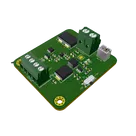
Brave is a versatile and efficient power board that can provide 12v, 5v and 3.3v outputs for various applications. It can be powered by battery or solar panel, and the battery can be recharged by solar energy. It can also be powered by a USB port if needed. This board is ideal for IoT projects that require reliable and stable power supply in different environments.
#IoT #power #management #usb
Properties
Properties describe core aspects of the project.
Pricing & Availability
Distributor | Qty 1 |
|---|---|
Arrow | $0.86–$2.41 |
Digi-Key | $0.72–$2.81 |
LCSC | $1.73–$3.46 |
Mouser | $2.91–$3.54 |
Verical | $0.50–$1.90 |
Assets

power_manager_board-removebg-preview.png
power_manager_board-removebg-previewThumbnail
qrcode.svg
qrcodeflux logo.svg
flux logoDefault
qrcodev2.svg
qrcodev2
power manager board.png
power manager boardControls
Welcome 👋
Flux helps you build PCBs faster with an AI teammate!
Create your account to collaborate, stay updated, fork your own version, and get instant answers from our AI agent.
collinsemasi
copilot
collinsemasi
copilot
Table