Project Cover Page

Can you help me make this the cover page of the project?
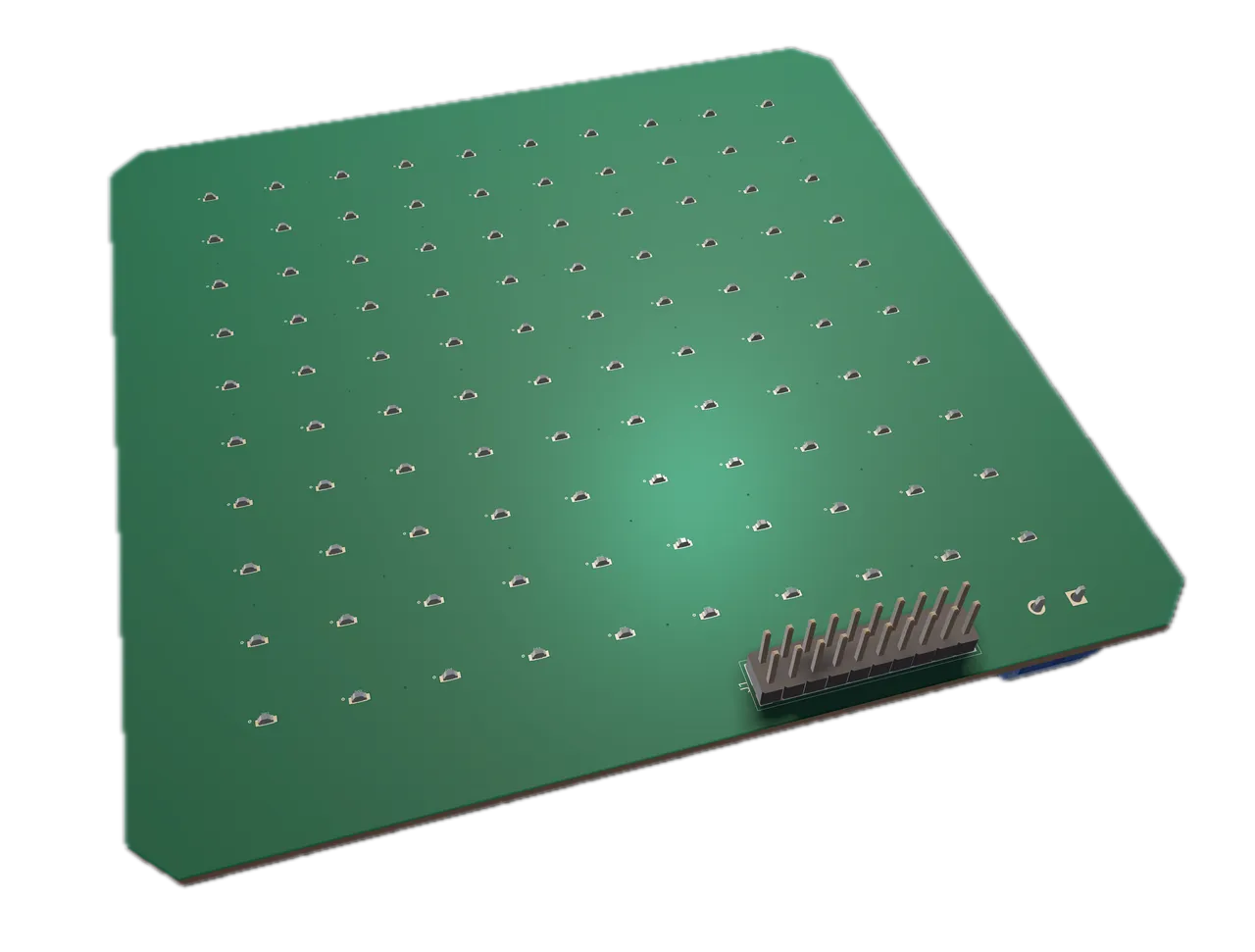
Image
Worked for 2 mins 15 sec
The PCB render is now set as the 10x10 LED Matrix project cover image and verified successfully.
Review, optimize, export
Run design review
Optimize PCB placement
Check power integrity
Prepare manufacturing files
Can you make the PC be a different color? Do I have to do that manually?
Can you make the board a different color?
Refine this doc
Ask about this doc
Design Notes
LED Matrix Drive
- Topology: common-anode rows with P-channel MOSFET high-side switches and constant-current column sinks.
- Row decoder outputs are active-low; each selected output pulls one MOSFET gate low.
- 100 kΩ gate-to-source resistors keep rows off if the decoder is unpowered or disconnected.
- 470 Ω series resistors limit 74HCT154 peak gate-charge current and damp switching edges.
- BLANK and ROW_ENABLE_N are pulled up to local +5 V so the display remains disabled if the controller is absent.
Driver Current Programming
- STP16CP05 datasheet table specifies approximately 20 mA per channel with R-EXT ≈ 1.006 kΩ.
- Use 1.00 kΩ, 1% on each driver.
Power Budget
- LED peak: 10 columns × 20 mA = 200 mA.
- Logic and driver allowance: approximately 50 mA.
- Design peak estimate: 250 mA at 5 V.
- Input PTC: 500 mA hold rating.
Multiplexing Sequence
- Assert OE/BLANK to disable column sinks.
- Disable row decoder or select a non-display address.
- Shift 32 bits through the cascaded drivers.
- Pulse LATCH.
- Set ROW_A[3:0] to 0–9.
- Enable the decoder.
- Deassert OE/BLANK for the desired dwell time.
- Repeat for the next row.
Use 2–5 µs dead time after disabling the old row and after enabling the new row during initial firmware bring-up. Shift all 32 bits every update and force unused outputs off.
External Interface Protection
- DATA, CLK, LATCH, BLANK, ROW_A0–ROW_A3, and ROW_ENABLE_N each use 4.7 kΩ series protection.
- SDO_OUT uses a 3.3 kΩ / 6.8 kΩ divider, producing approximately 3.37 V from a 5 V high level.
- The external controller should not actively drive HIGH into an unpowered matrix board; use low or high-impedance states during power sequencing.
Open Layout Constraint
- LED centers must be placed on a 10 mm × 10 mm grid during the PCB-layout phase.
LED Matrix Drive
Driver Current Programming
Power Budget
Multiplexing Sequence
External Interface Protection
Open Layout Constraint