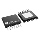
Part Information Review
Thought for 1 sec
- Set VS's Pin Type to "Power In"
- Set VS's Section to "Power"
- Set VS's Pin Group to "VS"
- Set VS's Pin Description to "Supply Input"
- Set VS's Pin Orientation to "Top"
- Set VS's Pin Type to "Power In"
- Set VS's Section to "Power"
- Set VS's Pin Group to "VS"
- Set VS's Pin Description to "Supply Input"
- Set VS's Pin Orientation to "Top"
- Set VS's Pin Type to "Power In"
- Set VS's Section to "Power"
- Set VS's Pin Group to "VS"
- Set VS's Pin Description to "Supply Input"
- Set VS's Pin Orientation to "Top"
- Set VOUT's Pin Type to "Power Out"
- Set VOUT's Section to "Output"
- Set VOUT's Pin Group to "VOUT"
- Set VOUT's Pin Description to "Load Output"
- Set VOUT's Pin Orientation to "Right"
- Set VOUT's Pin Type to "Power Out"
- Set VOUT's Section to "Output"
- Set VOUT's Pin Group to "VOUT"
- Set VOUT's Pin Description to "Load Output"
- Set VOUT's Pin Orientation to "Right"
- Set VOUT's Pin Type to "Power Out"
- Set VOUT's Section to "Output"
- Set VOUT's Pin Group to "VOUT"
- Set VOUT's Pin Description to "Load Output"
- Set VOUT's Pin Orientation to "Right"
- Set GND's Pin Type to "Ground"
- Set GND's Section to "Ground"
- Set GND's Pin Group to "GND"
- Set GND's Pin Description to "Device Ground"
- Set GND's Pin Orientation to "Bottom"
- Set GND's Pin Type to "Ground"
- Set GND's Section to "Ground"
- Set GND's Pin Group to "GND"
- Set GND's Pin Description to "Thermal Ground Pad"
- Set GND's Pin Orientation to "Bottom"
- Set EN's Pin Type to "Input"
- Set EN's Section to "Control"
- Set EN's Pin Group to "Control"
- Set EN's Pin Description to "Enable Input"
- Set EN's Pin Orientation to "Left"
- Set DIAG_EN's Pin Type to "Input"
- Set DIAG_EN's Section to "Control"
- Set DIAG_EN's Pin Group to "Control"
- Set DIAG_EN's Pin Description to "Diagnostics Enable"
- Set DIAG_EN's Pin Orientation to "Left"
- Set LATCH's Pin Type to "Input"
- Set LATCH's Section to "Control"
- Set LATCH's Pin Group to "Control"
- Set LATCH's Pin Description to "Latch Control"
- Set LATCH's Pin Orientation to "Left"
- Set ILIM's Pin Type to "Input"
- Set ILIM's Section to "Control"
- Set ILIM's Pin Group to "Control"
- Set ILIM's Pin Description to "Current Limit Set"
- Set ILIM's Pin Orientation to "Left"
- Set *FAULT's Pin Type to "Output"
- Set *FAULT's Section to "Diagnostic"
- Set *FAULT's Pin Group to "Diagnostic"
- Set *FAULT's Pin Description to "Fault Indicator"
- Set *FAULT's Pin Orientation to "Right"
- Set SNS's Pin Type to "Output"
- Set SNS's Section to "Diagnostic"
- Set SNS's Pin Group to "Diagnostic"
- Set SNS's Pin Description to "Current Sense Output"
- Set SNS's Pin Orientation to "Right"
- Set NC's Pin Type to "Not Connected"
- Set NC's Section to "No Connect"
- Set NC's Pin Group to "NC"
- Set NC's Pin Description to "No Connect"
- Set NC's Pin Orientation to "Right"
Refine this doc
Ask about this doc
TPS1HTC30-Q1 Pin Functional Groups
Source: TI TPS1HTC30-Q1 datasheet, Section 5 “Pin Configuration and Functions” for PWP / HTSSOP-14 package.
Each physical pin is assigned to exactly one functional group below. Repeated electrical functions such as VS and VOUT are grouped together, but no pin number is duplicated across groups.
Table
| Functional Group | Pins | Pin Names | Suggested Section | Suggested Pin Group | Suggested Flux Pin Type | Notes |
|---|---|---|---|---|---|---|
| Power Input / Supply | 12, 13, 14 | VS | Power | VS / Power | Power In | Main device supply input pins. Group all three together. |
| Power Output / Load Output | 8, 9, 10 | VOUT | Output / Signal | VOUT / Output | Power Out | High-side switch output pins to the load. Group all three together. |
| Ground / Thermal Return | 1, Thermal Pad | GND, GND thermal pad | Ground | GND / Ground | Ground | Device ground and exposed thermal pad. The thermal pad is internally shorted to ground and should be grouped with ground, not as a separate signal function. |
| Logic / Control Inputs | 2, 3, 5, 7 | EN, DIAG_EN, LATCH, ILIM | Control | Control | Input | Enable, diagnostics enable, thermal latch behavior select, and adjustable current-limit configuration. |
| Diagnostic Outputs | 4, 6 | FAULT, SNS | Signal / Diagnostic | Diagnostic | Output | FAULT is an open-drain fault output; SNS is the current-sense / diagnostic analog output. |
| No Connect | 11 | NC | No Connect | NC | Not Connected | No internal connection; do not reuse this pin in another group. |
Recommended Non-Duplicated Grouping
- Power Input: VS pins 12, 13, 14
- Vout / Load Output: VOUT pins 8, 9, 10
- Gnd: GND pin 1 and exposed thermal pad
- Control: EN pin 2, DIAG_EN pin 3, LATCH pin 5, ILIM pin 7
- Diagnostics: FAULT pin 4, SNS pin 6
- No Connect: NC pin 11
Notes
- Do not put the same physical pin into both “Power” and “Gnd”; for this part, I recommend keeping supply input, output, and ground as separate functional groups because they serve different electrical roles.
- If Flux requires a broader Section field, use: Power for VS, Signal/Output for VOUT, Ground for GND/thermal pad, Control for EN/DIAG_EN/LATCH/ILIM, Signal/Diagnostic for FAULT/SNS, and No Connect for NC.
- If Flux requires a Pin Group field, use the specific names above: VS, VOUT, GND, Control, Diagnostic, NC.
Recommended Non-Duplicated Grouping
Notes