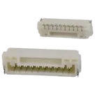
Part Metadata Review and Update
Thought for 2 mins 37 sec
Part audit complete
1) Available part information
2) Datasheet URL status
Electrical characteristics
Absolute maximum style limits available in datasheet
Recommended operating / application conditions
Pin / circuit information
Pin descriptions
Mechanical / package dimensions
Special features / notes
4) Cross-check: schematic symbol and footprint vs datasheet
Match assessment
Issues that should be flagged
Manufacturing-risk conclusion
Bottom line
Table
| Field | Result |
|---|---|
| Project name | SM10B-GHS-TB_LF__SN_ |
| Manufacturer | JST |
| MPN | SM10B-GHS-TB(LF)(SN) |
| Part type | Connector |
| Mount | Surface Mount |
| Description | Connector Header Surface Mount, Right Angle, 10 position, 1.25 mm pitch |
| Datasheet URL present | Yes |
| Datasheet source used | |
| Functional family from datasheet | GH series, wire-to-board, crimp style, side-entry / top-entry family |
| Position count for this MPN | 10 circuits |
| Schematic implementation | 12 separate terminals total: 10 signal circuits + 2 reinforcement tabs |
| Footprint asset | SM10BGHSTBLFSN.kicad_mod |
| 3D model asset | SM10B-GHS-TB.STEP |
A datasheet URL was already set, so no web lookup or property update was required.
3) Datasheet scan summary
Product metadata
Table
| Parameter | Datasheet value |
|---|---|
| Series | GH CONNECTOR |
| Connector type | Wire-to-board, crimp style |
| Header style | SMT, side entry type |
| Pitch | 1.25 mm |
| Circuits | 10 |
| Locking | Secure locking function / large outer latch |
| Compliance | RoHS2 |
| Packaging | Embossed taping, 2,500 headers per reel |
Table
| Parameter | Datasheet value |
|---|---|
| Current rating | 1.0 A AC/DC (AWG #26) |
| Voltage rating | 50 V AC/DC |
| Contact resistance, initial | 30 mΩ max. |
| Contact resistance, after test | 50 mΩ max. |
| Insulation resistance | 100 MΩ min. |
| Dielectric withstanding voltage | 500 VAC for one minute, no breakdown or flashover |
This connector datasheet does not present a separate semiconductor-style “Absolute Maximum Ratings” table. The practical published limits are:
Table
| Limit | Datasheet value |
|---|---|
| Maximum rated current | 1.0 A AC/DC |
| Maximum rated voltage | 50 V AC/DC |
| Temperature range | -40°C to +105°C |
Table
| Item | Datasheet value |
|---|---|
| Operating temperature range | -40°C to +105°C |
| Intended use | Internal connections in electrical/electronic equipment for high density applications |
| PCB pattern pitch tolerance | ±0.05 and shall not accumulate |
| PCB layout note | Layout is viewed from the connector mounting surface |
Table
| Item | Datasheet value |
|---|---|
| Circuit numbering | No. 1 circuit is explicitly identified |
| Circuit count to header mapping | 10 circuits -> SM10B-GHS-TB |
| Reinforcement tabs | Header material list includes reinforcement: copper alloy, tin-plated |
| Contact family | SSHL-002T-P0.2 |
| Applicable wire | AWG #30 to #26, insulation O.D. 0.76 to 1.0 mm |
This datasheet does not provide unique electrical pin names beyond circuit numbering. For this part, the meaningful descriptions are:
Table
| Pin class | Meaning |
|---|---|
| Circuits 1-10 | Signal/contact positions of the 10-circuit header |
| Reinforcement tabs | Mechanical hold-down / solder anchor tabs |
Table
| Parameter | Datasheet value |
|---|---|
| Entry style | Side entry |
| A dimension for 10 circuits | 11.25 mm |
| B dimension for 10 circuits | 15.75 mm |
| Height | 5.7 mm |
| Depth figures shown | 4.25 mm / 4.05 mm |
| PCB land width for signal pads | 0.6 ±0.05 mm |
| Pitch | 1.25 ±0.05 mm |
| Mechanical tab pad width | 1.0 ±0.1 mm |
| Signal pad length figure shown | 1.35 ±0.1 mm |
| Side-entry layout dimensions shown | 2.7 ±0.1 mm, 3.7 ±0.1 mm, 5.4 ±0.1 mm |
Table
| Feature | Datasheet note |
|---|---|
| Mating security | Secure lock mechanism |
| Anti-mismatch | Housing designed to prevent incorrect mating |
| Contact protection | Structured to prevent contact deformation |
| Finish | Tin-plated copper alloy contacts |
| Resin materials | Housing: PBT; header base housing: heat-resistant PA |
| Important note | Specifications registered to overseas standards may differ from general specifications |
Table
| Area | Result | Notes |
|---|---|---|
| MPN | Pass | Project MPN matches datasheet part family and 10-circuit side-entry header. |
| Position count | Pass | 10 signal circuits are present. |
| Mechanical tabs included | Pass | 2 extra SMT pads exist and align with reinforcement tabs. |
| Footprint pitch | Pass | Footprint uses 1.25 mm pitch for pads 1-10. |
| Signal pad width | Pass | Footprint uses 0.600 mm, matching datasheet. |
| Mechanical tab pad width | Pass | Footprint uses 1.000 mm, matching datasheet. |
| Side-entry geometry | Pass | Footprint dimensions align with side-entry style, not top-entry style. |
| Datasheet orientation note | Needs care | Datasheet layout is viewed from mounting surface; footprint appears consistent, but this is a common source of mirrored footprints if manually recreated. |
| Symbol pin metadata | Issue | Pin names/descriptions are effectively undefined in the current schematic representation. |
| Symbol structure | Issue | The part is represented as separate terminal elements rather than one unified connector symbol. |
| Electrical pin typing | Issue | All pins are marked Unspecified. |
| Designator consistency | Minor issue | Project designator prefix is J, while internal terminal elements show P prefix metadata. |
Table
| Severity | Finding | Risk |
|---|---|---|
| High | The schematic symbol is not a conventional single 10-pin connector symbol; it is split into separate terminal elements plus two mounting tabs. | Easier to miswire, harder to review, and higher risk of pin-order mistakes during reuse. |
| Medium | Pin names are undefined and pin types are unspecified. | ERC quality is reduced; users may connect the wrong circuit because only numbers are visible. |
| Medium | Reinforcement tabs are present, but they are not clearly differentiated as mechanical-only in the symbol metadata. | A user could mistakenly treat them as signal pins in the part definition workflow. |
| Low | Designator-prefix metadata is inconsistent between project-level connector identity and internal terminal elements. | Mostly a library cleanliness issue, but can create confusion in generated symbols/docs. |
Table
| Category | Conclusion |
|---|---|
| Wrong part ordered | Low risk if the MPN is used directly, because the MPN and package family align. |
| Footprint manufacturing failure | Low risk based on the extracted pad geometry; the footprint appears consistent with the datasheet side-entry land pattern. |
| Board assembly / fit issue | Low risk from the footprint itself, assuming the side-entry orientation is what you intended. |
| Board failure due to symbol mismatch | Medium risk at the design-entry stage, because the symbol metadata is weak and can enable wiring mistakes. |
- The footprint looks consistent with the JST datasheet for SM10B-GHS-TB(LF)(SN).
- The main problems are symbol quality and metadata quality, not the copper land pattern.
- The biggest improvements would be:
- Convert the symbol into one unified 10-circuit connector symbol
- Mark the 2 reinforcement tabs as mechanical / non-signal
- Give pins explicit names/descriptions
- Set appropriate pin electrical types
If you want, I can next check whether I’m able to clean up the part metadata and symbol structure for this part project.
@file inspect pin mapping
Create cleaner connector
Check part metadata