Part Review and Datasheet Update
Worked for 4 mins 12 sec
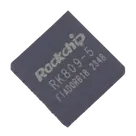
Completed the RK809-5 part review and added the datasheet/metadata to the project properties. I created the full detailed report here: RK809-5 Part Review.
Key flags: the QFN-68-EP(7x7) footprint and 69-pad count match the datasheet, but pins 42/43 are named
MIC1N/MIC1P while the datasheet table uses MICIN/MICIP, and most pins still have unspecified pin types/descriptions. The footprint uses a single large exposed-pad paste area; I’d recommend segmented paste and board-level thermal vias for robust assembly/thermal performance.
Set the pin type and datasheet-based pin description for every terminal. Group all terminals into logical symbol sections according to their functions and the datasheet recommendations. Ensure that pin names, pin numbers, pin types, descriptions, and section assignments are fully consistent with the official datasheet.
Worked for 17 sec
I’ll update every RK809-5 terminal with datasheet pin type, pin description, and section assignment, rename the microphone pins to the datasheet table names, then verify the terminal set afterward.
Worked for 3 mins 9 sec
Done. I updated all 69 RK809-5 terminals with datasheet-based pin numbers, standard pin types, pin descriptions, and single logical section assignments.
I also renamed
MIC1N → MICIN and MIC1P → MICIP to match the official datasheet pin table. Verification passed for terminal, terminal pin-number, and missing-property part review checks with no open warnings/errors.Update review report
Check footprint mapping
Run full review
Improve EPAD footprint
Refine this doc
Ask about this doc
RK809-5 Part Review
Date: 2026-06-08
Scope
Reviewed the RK809-5 part project metadata, schematic symbol terminals, PCB footprint pads, and available datasheet information.
Source Information
- MPN: RK809-5
- Manufacturer: Rockchip
- Description: Power-management IC (PMIC) with integrated audio codec, RTC, power sequencing, load switches, and battery fuel gauge
- Package: QFN-68 with exposed pad, 7 mm x 7 mm, 0.35 mm pitch
- Datasheet used: Rockchip RK809 Datasheet Rev 2.4, Jan. 2024
- Datasheet URL recorded in project properties: https://rockchip.fr/RK809%20datasheet%20V2.4.pdf
- Distributor corroboration: LCSC/JLCPCB list RK809-5 as Rockchip C2939628, QFN-68-EP(7x7), Power Management - Specialized, RoHS.
Key Datasheet Specs
- Input range: 2.7 V to 5.5 V
- Standby current: 35 uA typical stated feature
- Buck converters:
- BUCK1: 0.5 V to 2.4 V, 2.5 A max
- BUCK2: 0.5 V to 2.4 V, 2.5 A max
- BUCK3: 0.5 V to 2.4 V or resistor-divider mode, 1.5 A max
- BUCK4: 0.5 V to 3.4 V, 1.5 A max
- BUCK5: 1.5 V to 3.6 V, 2.5 A max
- LDOs:
- LDO1, LDO2, LDO4-LDO9: 0.6 V to 3.4 V, 400 mA max
- LDO3: 0.6 V to 3.4 V, 100 mA max, high PSRR 75 dB at 1 kHz
- Load switches:
- Switch1: 2.1 A max, Rds(on) 90 mohms
- Switch2: 2.1 A max, Rds(on) 100 mohms
- Battery fuel gauge: separate 16-bit battery voltage ADC and 16-bit battery current ADC, OCV plus coulomb-counter algorithm
- RTC: 32.768 kHz crystal oscillator support and 32.768 kHz output buffer
- Audio:
- 24-bit ADC and DAC
- I2S/PCM interface, 48 kHz to 192 kHz sample rate
- Differential or single-ended microphone input
- Real-ground Class-AB headphone driver for 32 ohm load
- Class-D speaker driver, 1.3 W into 8 ohm BTL load from 5 V
- Recommended operating ranges:
- General supply / power / logic groups: up to 5.5 V, as grouped in datasheet
- Low-voltage analog pins SNSP, SNSN, VREF, VCC_1P8D, VCC_1P8A, MIC1N/MIC1P: -0.2 V to 1.98 V
- Headphone pins: -2.7 V to +2.7 V
- Charge-pump positive pins: -0.3 V to 2.7 V
- Charge-pump negative pins: -2.7 V to 0.3 V
- Power dissipation: 2 W max
- Absolute maximum ratings include 6.5 V max for main power/logic groups, 1.98 V max for low-voltage analog group, and -40 C to 125 C operating junction temperature.
Symbol / Pin Review
The project contains 69 terminal components corresponding to pins 1-68 plus exposed pad. Pin numbers and terminal names match the RK809 pin table/assignment for the QFN68 package, with the exception noted below.
Verified Pin Mapping
- Pins 1-41 match the datasheet sequence: SCL, SDA, LDO7, VCC7, LDO8, LDO9, INT, FB2, SW2, VCC2, VCC1, SW1, FB1, LRCLK, BCLK, MCLK, SDI, SDO/PDMDATA, PDMCLK, LDO3, LDO2, VCC5, LDO1, VCC3, SW3, VBUCK3, FB3, LDO4, LDO5, VCC6, LDO6, SPKP_OUT, VCC_SPK_HP, SPKN_OUT, VCC_CPVSS, CPN, CPP, VCC_CPVDD, HPL_OUT, HP_SNS, HPR_OUT.
- Pins 44-68 match the datasheet sequence: VCC_1P8A, VCC_RTC, VREF, GNDREF, VCC_1P8D, SLEEP, XIN, XOUT, PWRON, SW5, VCC9, SWOUT1, BATDIV, VCC8, SWOUT2, FB5, EXT_EN, VDC, SNSP, SNSN, FB4, SW4, VCC4, RESETB, CLK32K.
- Exposed pad is present as EPAD / pin 69 and maps to exposed ground.
Flagged Symbol Mismatch / Ambiguity
- Pins 42 and 43 are named MIC1N and MIC1P in the Flux symbol. The datasheet pinout table names these pins MICIN and MICIP, with descriptions "Negative input of the Microphone" and "Positive input of the Microphone." The datasheet pin-assignment figure/OCR also shows MIC1P in one location, so this may be a naming convention/OCR inconsistency rather than an electrical pinout error. Recommendation: rename the symbol pins to the exact datasheet-table names MICIN and MICIP, or add pin descriptions clarifying the aliases MIC1N/MIC1P = MICIN/MICIP.
Missing Symbol Metadata
- All terminals currently have Pin Type set to Unspecified.
- Terminal-level Pin Description properties are not populated, aside from the terminal designator itself.
- Recommendation: populate Pin Type and Pin Description from the datasheet table. This will improve ERC behavior and make the part safer to reuse.
Footprint Review
- Footprint asset name: QFN35P700X700X80-69N-D.kicad_mod
- Datasheet package: QFN68, 7 mm x 7 mm, exposed pad, 0.35 mm pitch
- Footprint body/fab outline: 7.0 mm x 7.0 mm
- Lead pitch: 0.35 mm, matching datasheet
- Peripheral pad width: 0.15 mm, matching nominal datasheet lead width b = 0.15 mm
- Peripheral pad length: 0.85 mm. Datasheet lead length L is 0.30 to 0.50 mm; land pattern pads are normally longer than package leads for solder fillet, so this is plausible.
- Exposed pad: 5.59 mm x 5.59 mm. Datasheet exposed-pad max is 5.59 mm, nominal 5.49 mm. The footprint uses the max exposed-pad size.
- Pad count: 68 peripheral pads plus exposed pad = 69 pads, matching project context and package.
Flagged Footprint Considerations
- The exposed pad is modeled as a single 5.59 mm square paste/mask/copper pad. For manufacturability, consider segmented solder paste windows on the EPAD to reduce voiding and floating during reflow.
- No thermal via array was observed in the part footprint data. For applications near the 2 W dissipation limit or using multiple high-current bucks/speaker amp, add thermal vias in the board design under/near EPAD tied to ground.
Overall Result
- Datasheet URL and key metadata were added to project-level properties.
- Pin count and footprint geometry are consistent with the RK809 QFN68 7x7 package.
- Primary mismatch: microphone pins use MIC1N/MIC1P in the symbol while the datasheet table uses MICIN/MICIP.
- Primary metadata gap: Pin Type and Pin Description are mostly unspecified and should be filled from the datasheet for a production-quality library part.


Welcome 👋
Flux accelerates your PCB design with AI.
Create your account to start using this component and bring your ideas to life.