Part Review and Datasheet Verification
5:05
Evalu.
Organ.
Following.
Using Schematic Tool.
Using PCB Layout Tool.
Looking for "Part numbering key and ordering information for QSH series, including what -030, -01, -L, -D, -A options mean" in qsh.pdf
Looking for "Positions or total number of contacts for QSH-030; contacts per row and total contacts" in qsh.pdf
Looking for "Pitch specification and row-to-row spacing for QSH series connectors" in qsh.pdf
Looking for "Mechanical dimensions drawing for QSH-030 with overall length and width; reference footprint dimensions" in qsh.pdf
Looking for "Recommended PCB land pattern (footprint) for QSH-030-01-L-D-A" in qsh.pdf
Looking for "Pin numbering convention and row labeling (A/B) for QSH series; where pin 1 is located" in qsh.pdf
Looking for "Mating connector series and stack height options for QSH" in qsh.pdf
Looking for "Electrical characteristics: current rating per contact, voltage rating, insulation resistance, dielectric withstanding voltage, contact resistance" in qsh.pdf
Looking for "Operating temperature range and storage temperature for QSH connectors" in qsh.pdf
Looking for "Special features such as alignment pins, polarization, shield, ground blade, guideposts for QSH" in qsh.pdf
Looking for "Soldering and reflow recommendations for QSH series (peak temperature, profiles)" in qsh.pdf
Looking for "Packaging information: tape and reel or tray for -01 or -A options" in qsh.pdf
Looking for "Absolute maximum ratings or environmental ratings (if any) for QSH series" in qsh.pdf
Looking for "Connector height (mated and unmated), stack height achieved with QTH/QSH" in qsh.pdf
Looking for "Footprint pad count per position and any keepout or solder mask recommendations" in qsh.pdf
Looking for "Meaning of the -A suffix in QSH-XXX-XX-XX-X-XXX; what does -A denote?" in qsh.pdf
Looking for "Location of pin 1 and row labeling for QSH; figure showing A and B rows and numbering sequence" in qsh.pdf
Looking for "Recommended PCB land pattern dimensions per pad for QSH; pad size and spacing details" in qsh.pdf
- Available part information (from the part project)
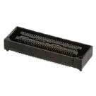
- MPN: QSH-030-01-L-D-A
- Manufacturer: Samtec
- Part type: Connectors
- Mount: Surface Mount
- Designator prefix: J
- Description: “Samtec QSH Series 0.5mm Pitch 60 Way 2 Row Straight PCB Socket, Surface Mount, Solder Termination”
- Datasheet: https://suddendocs.samtec.com/catalog_english/qsh.pdf
- Datasheet URL presence and update
- A datasheet URL is already set on this part. No update required.
- Datasheet metadata extraction (QSH series; specific to -030, -01, -L, -D, -A where available)
- Series: QSH
- Positions per row: 30 (code “030”) → total contacts: 60 (2 rows)
- Lead style: 01
- Plating: L = 10 µin (0.25 µm) Gold on contact, Matte Tin on tail
- Type: D = Single-ended (not differential-pair)
- Option: A = Pick & place pad (polyimide film)
- Pitch: 0.50 mm (0.0197 in)
- Rows: 2 (A/B)
- Current rating: 2 A per contact (with 2 pins powered)
- Ground plane current (if applicable in options using ground plane): 25 A per ground plane (1 ground plane powered)
- Voltage rating: 175 VAC / 247 VDC
- Operating temperature range: -55 °C to +125 °C
- General series dimensions include typical widths/heights such as (3.05) 0.120, (3.25) 0.128, (7.24) 0.285, (7.49) 0.295, etc. (see drawing)
- Mated stack height with QTH (by QTH lead style):
- 01: A height 4.27 mm; with QSH 5.00 mm
- 02: 7.26 mm; with QSH 8.00 mm
- 03: 10.27 mm; with QSH 11.00 mm
- 04: 15.25 mm; with QSH 16.00 mm
- 05: 18.26 mm; with QSH 19.00 mm
- 07: 24.24 mm; with QSH 25.00 mm
- 09: 13.26 mm; with QSH 14.00 mm
- Note: Processing conditions can affect mated height.
- The datasheet provides a full recommended layout for QSH-XXX-01-X-D-XXX including typical values such as:
- 0.5001 mm pitch (0.01969 in)
- Repeating dimensions like 0.279 mm, 0.815 mm, 6.20 mm, 14.504 mm, 4.890 mm, etc.
- Symmetry about the centerline and connector envelope keep-out notes
- For -SD/-DS (screw-down) options, a different application drawing is referenced
- Soldering guidance (per Samtec SMT process guidance): connectors typically must withstand up to 230 °C for 30–60 s, and may see up to 260 °C for 10 s (refer to Samtec processing docs)
- QSH has two rows (A and B) at 0.50 mm pitch. QSH-030-D = 30 contacts per row → total 60 contacts.
- The catalog page is largely graphical; explicit text for “Pin 1 locator” could not be extracted from the text layer. Conventionally, rows are labeled A/B, with numbering sequence shown in the figure on the page.
- Board mate: QTH (QTH/QSH system)
- Cable mates: HQCD, HQDP
- Cross-check: schematic symbol and footprint vs datasheet
-
Total contacts mismatch (critical):
- Datasheet for QSH-030-D: 2 rows, 30 contacts per row → total contacts: 60.
- Schematic symbol contains 64 terminals (components labeled as “Terminal” with designators 1..64; no nets yet).
- Footprint contains 64 pads (Pads 1..64 in the PCB node tree).
- Impact: This is a high-risk mismatch. If left uncorrected, it can cause net mapping errors, assembly issues, and functional failures. The part is advertised as “60 Way 2 Row,” so symbol and footprint should present exactly 60 signal pads (30 per row), with any additional mechanical features (e.g., pick & place pad, mechanical holes) implemented as non-electrical features, not numbered contacts.
-
Row labeling and numbering:
- Datasheet: two rows (A/B) at 0.50 mm pitch; numbering figure is present.
- Current symbol: appears to use generic untyped “Terminal” objects numbered sequentially; there’s no explicit A/B row labeling or a clear pin 1 indication in the symbol.
- Risk: Ambiguity during schematic capture and layout correlation. Suggest adopting A/B row labels and confirming the correct numbering sequence/pin 1 location per the datasheet figure.
-
Pitch and land pattern:
- Datasheet: pitch is 0.50 mm and provides detailed recommended PCB layout for QSH-XXX-01-X-D-XXX.
- Current footprint: Pad count visible; specific pad sizes/spacing not displayed in the node index. Unable to verify actual pad pitch/geometry from available layout nodes alone.
- Action needed: Confirm pad pitch (should be 0.50 mm) and land pattern dimensions match the recommended PCB layout for QSH-XXX-01-X-D-XXX.
-
Option -A (Pick & place pad):
- Datasheet: “A” = pick & place pad (polyimide film).
- Footprint: From the node listing alone, additional non-electrical features (pick & place pad zone) aren’t visible. If modeled, it should not be implemented as numbered signal pads. Ensure the pick & place pad is handled as a mechanical/assembly feature, not as an electrical pad.
-
Soldering and mechanical holes:
- The catalog page references PTH features for certain variants/processes (paste-in-hole notes are present in the recommended layout text). For the -01 lead style single-ended variant (no screw-down), ensure any PTH or mechanical holes in the footprint exactly match the recommended layout for this specific option and are not misrepresented as electrical pads.
- Reduce the symbol to exactly 60 signal pins (30 per row) and align numbering with the datasheet’s A/B row scheme and pin 1 orientation.
- Reduce the footprint to exactly 60 electrical pads for signals; represent any mechanical features (pick & place pad, optional holes) as non-electrical/mechanical where appropriate.
- Verify pad pitch is exactly 0.50 mm and all pad and spacing dimensions match the “RECOMMENDED PCB LAYOUT FOR QSH-XXX-01-X-D-XXX.”
- Add a clear pin 1 locator on the symbol and footprint silkscreen/assembly layers per the datasheet figure.
Ready.
Reviews

- Wirelessly connects nets on schematic. Used to organize schematics and separate functional blocks. To wirelessly connect net portals, give them same designator. #portaljharwinbarrozo43.0M
- Wirelessly connects power nets on schematic. Identical to the net portal, but with a power symbol. Used to organize schematics and separate functional blocks. To wirelessly connect power net portals, give them the same designator. #portal #powerjharwinbarrozo11.4M
- A generic fixed resistor for rapid developing circuit topology. Save precious design time by seamlessly add more information to this part (value, footprint, etc.) as it becomes available. Standard resistor values: 1.0Ω 10Ω 100Ω 1.0kΩ 10kΩ 100kΩ 1.0MΩ 1.1Ω 11Ω 110Ω 1.1kΩ 11kΩ 110kΩ 1.1MΩ 1.2Ω 12Ω 120Ω 1.2kΩ 12kΩ 120kΩ 1.2MΩ 1.3Ω 13Ω 130Ω 1.3kΩ 13kΩ 130kΩ 1.3MΩ 1.5Ω 15Ω 150Ω 1.5kΩ 15kΩ 150kΩ 1.5MΩ 1.6Ω 16Ω 160Ω 1.6kΩ 16kΩ 160kΩ 1.6MΩ 1.8Ω 18Ω 180Ω 1.8KΩ 18kΩ 180kΩ 1.8MΩ 2.0Ω 20Ω 200Ω 2.0kΩ 20kΩ 200kΩ 2.0MΩ 2.2Ω 22Ω 220Ω 2.2kΩ 22kΩ 220kΩ 2.2MΩ 2.4Ω 24Ω 240Ω 2.4kΩ 24kΩ 240kΩ 2.4MΩ 2.7Ω 27Ω 270Ω 2.7kΩ 27kΩ 270kΩ 2.7MΩ 3.0Ω 30Ω 300Ω 3.0KΩ 30KΩ 300KΩ 3.0MΩ 3.3Ω 33Ω 330Ω 3.3kΩ 33kΩ 330kΩ 3.3MΩ 3.6Ω 36Ω 360Ω 3.6kΩ 36kΩ 360kΩ 3.6MΩ 3.9Ω 39Ω 390Ω 3.9kΩ 39kΩ 390kΩ 3.9MΩ 4.3Ω 43Ω 430Ω 4.3kΩ 43KΩ 430KΩ 4.3MΩ 4.7Ω 47Ω 470Ω 4.7kΩ 47kΩ 470kΩ 4.7MΩ 5.1Ω 51Ω 510Ω 5.1kΩ 51kΩ 510kΩ 5.1MΩ 5.6Ω 56Ω 560Ω 5.6kΩ 56kΩ 560kΩ 5.6MΩ 6.2Ω 62Ω 620Ω 6.2kΩ 62KΩ 620KΩ 6.2MΩ 6.8Ω 68Ω 680Ω 6.8kΩ 68kΩ 680kΩ 6.8MΩ 7.5Ω 75Ω 750Ω 7.5kΩ 75kΩ 750kΩ 7.5MΩ 8.2Ω 82Ω 820Ω 8.2kΩ 82kΩ 820kΩ 8.2MΩ 9.1Ω 91Ω 910Ω 9.1kΩ 91kΩ 910kΩ 9.1MΩ #generics #CommonPartsLibraryjharwinbarrozo1.5M
- A generic fixed capacitor ideal for rapid circuit topology development. You can choose between polarized and non-polarized types, its symbol and the footprint will automatically adapt based on your selection. Supported options include standard SMD sizes for ceramic capacitors (e.g., 0402, 0603, 0805), SMD sizes for aluminum electrolytic capacitors, and through-hole footprints for polarized capacitors. Save precious design time by seamlessly add more information to this part (value, footprint, etc.) as it becomes available. Standard capacitor values: 1.0pF 10pF 100pF 1000pF 0.01uF 0.1uF 1.0uF 10uF 100uF 1000uF 10,000uF 1.1pF 11pF 110pF 1100pF 1.2pF 12pF 120pF 1200pF 1.3pF 13pF 130pF 1300pF 1.5pF 15pF 150pF 1500pF 0.015uF 0.15uF 1.5uF 15uF 150uF 1500uF 1.6pF 16pF 160pF 1600pF 1.8pF 18pF 180pF 1800pF 2.0pF 20pF 200pF 2000pF 2.2pF 22pF 20pF 2200pF 0.022uF 0.22uF 2.2uF 22uF 220uF 2200uF 2.4pF 24pF 240pF 2400pF 2.7pF 27pF 270pF 2700pF 3.0pF 30pF 300pF 3000pF 3.3pF 33pF 330pF 3300pF 0.033uF 0.33uF 3.3uF 33uF 330uF 3300uF 3.6pF 36pF 360pF 3600pF 3.9pF 39pF 390pF 3900pF 4.3pF 43pF 430pF 4300pF 4.7pF 47pF 470pF 4700pF 0.047uF 0.47uF 4.7uF 47uF 470uF 4700uF 5.1pF 51pF 510pF 5100pF 5.6pF 56pF 560pF 5600pF 6.2pF 62pF 620pF 6200pF 6.8pF 68pF 680pF 6800pF 0.068uF 0.68uF 6.8uF 68uF 680uF 6800uF 7.5pF 75pF 750pF 7500pF 8.2pF 82pF 820pF 8200pF 9.1pF 91pF 910pF 9100pF #generics #CommonPartsLibraryjharwinbarrozo1.5M
- A generic fixed inductor for rapid developing circuit topology. *You can now change the footprint and 3D model at the top level anytime you want. This is the power of #genericsjharwinbarrozo15.6k
- An electrical connector acting as reusable interface to a conductor and creating a point where external circuits can be connected.Terminal
- 47 kOhms ±5% 0.125W, 1/8W Chip Resistor 0805 (2012 Metric) Automotive AEC-Q200 Thick Film #forLedBlinkjharwinbarrozo1.2M
- 10uF Capacitor Aluminum Polymer 20% 16V SMD 5x5.3mm #forLedBlink #commonpartslibrary #capacitor #aluminumpolymer #radialcanjharwinbarrozo1.2M
- Yellow 595nm LED Indication - Discrete 1.7V 1206 (3216 Metric) #forLedBlinkjharwinbarrozo1.1M


Pricing & Availability
See prices from popular manufacturers for your project.
Assets

QSH-030-01-L-D-A-thumb.png
QSH-030-01-L-D-A-thumbThumbnailQSH-030-01-L-D-A
QSH-030-01-L-D-A.kicad_modFootprintQSH-030-01-L-D-A
QSH-030-01-L-D-A.stp3D Model
QSH-030-01-L-D-A
QSH-030-01-L-D-A Symbol.svgDefaultControls
Welcome 👋
Flux accelerates your PCB design with AI.
Create your account to start using this component and bring your ideas to life.