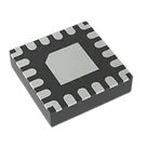
Part Review and Datasheet Update
Worked for 3 mins 7 sec
Review complete. I created the detailed report here: Part Review: PCM1822IRTER.
Open items:
- Datasheet URL was already populated, so I did not replace it.
- Main mismatch: the datasheet shows WQFN-20 plus one exposed VSS thermal pad, but the symbol/footprint currently exposes five extra VSS pins/pads numbered 21–25.
- Pin types/descriptions are mostly unset and should be populated from the datasheet.
Suggested next steps:
- Replace pins/pads 21–25 with one exposed pad terminal, pin 21 / VSS thermal pad.
- Update footprint to 20 perimeter pads + one central exposed pad per TI RTE0020A.
- Populate pin types and descriptions from the datasheet table.
- Optionally change
MountfromHardwareto SMD / surface mount.

Populate all pin types and descriptions from the datasheet table.
Thought for 5 sec
I’ll update each terminal’s Pin Type and Pin Description from the PCM1822 datasheet pin-function table, then verify the properties were applied.
Worked for 36 sec
Populated and verified Pin Type and Pin Description for all 25 current terminals from the PCM1822 datasheet table.
Open items:
- The current part still has five thermal-pad/VSS terminals numbered 21–25; the datasheet represents this as one exposed VSS thermal pad.
Suggested next steps:
- Normalize Pin Type values to Flux’s standard ERC options if desired.
- Replace VSS_5–VSS_9 with a single exposed-pad terminal/pad.
- Re-run the part review after the thermal pad cleanup.
Fix pad, types, review
Fix exposed pad
Normalize pin types
Verify footprint geometry
Run part review
Name
Pin #
Type
Part Type
Pin Description
Pin Orientation
IN1P
1
Analog input
Terminal
Analog input 1P pin.
IN1M
2
Analog input
Terminal
Analog input 1M pin.
IN2P
3
Analog input
Terminal
Analog input 2P pin.
IN2M
4
Analog input
Terminal
Analog input 2M pin.
VSS_1
5
Analog supply
Terminal
VSS analog supply/ground pin. Short this pin directly to the board ground plane.
Bottom
SDOUT
6
Digital output
Terminal
Audio serial data interface bus output.
BCLK
7
Digital I/O
Terminal
Audio serial data interface bus bit clock.
FSYNC
8
Digital I/O
Terminal
Audio serial data interface bus frame synchronization signal.
IOVDD
9
Digital supply
Terminal
Digital I/O power supply, nominal 1.8 V or 3.3 V.
VSS_2
10
Analog supply
Terminal
VSS analog supply/ground pin. Short this pin directly to the board ground plane.
Bottom
MD1
11
Digital input
Terminal
Device configuration mode select 1 pin.
MD0
12
Digital input
Terminal
Device configuration mode select 0 pin.
MSZ
13
Digital input
Terminal
Audio interface bus master or slave select pin.
DREG
14
Digital supply
Terminal
Digital regulator output voltage for digital core supply, nominal 1.5 V.
VSS_3
15
Analog supply
Terminal
VSS analog supply/ground pin. Short this pin directly to the board ground plane.
Bottom
AVDD
16
Analog supply
Terminal
Analog power supply, nominal 3.3 V.
AREG
17
Analog supply
Terminal
Analog on-chip regulator output voltage for analog supply, nominal 1.8 V.
VREF
18
Analog
Terminal
Analog reference voltage filter output.
PCM1822IRTER