Part Review and Datasheet Verification
add pin type and section for all the pins based on the datasheet.
Worked for 14 sec
I’ll update every terminal with datasheet-derived Pin Type and Section values, then re-read the schematic to verify the metadata landed correctly.
Worked for 1 min 41 sec
The first update landed, but the editor flagged non-standard Pin Type/Section labels. I’m normalizing them to the platform’s accepted values while preserving the datasheet intent.
Worked for 1 min 8 sec
Updated all 57 PCA9450CHNY terminals with datasheet-based
Pin Type and Section metadata, then verified the schematic.I normalized the values to accepted options: power pins are now
Power In/Power Out, ground pins are Ground, I/O pins are Input/Output/Bi-Directional, and open-drain outputs POR_B/IRQ_B are Open Collector. Sections are assigned by primary function: Voltage Regulator, Power, Reset, Clock, Enable, Control, and Interface.Fix naming mismatches
Add pin descriptions
Verify footprint geometry
Run part review
Update review document
Refine this doc
Ask about this doc
PCA9450CHNY Part Review
Source information
- Project part: PCA9450CHNY
- Manufacturer: NXP Semiconductors
- Official datasheet URL: https://www.nxp.com/docs/en/data-sheet/PCA9450.pdf
- Datasheet reviewed: PCA9450 Power management IC for i.MX 8M application processor family
- Project description: Power Management Specialized - PMIC PMIC for i.MX8M Plus(865S)
Available project metadata reviewed
- Project name / MPN: PCA9450CHNY
- Project description indicates PMIC for i.MX8M Plus.
- Schematic representation consists of 57 Terminal components, one per package pin/pad.
- Each terminal currently has:
- Part Type: Terminal
- Pin Type: Unspecified
- Pin Number: populated for pins 1-57
- Designator Prefix: P
- Layout contains 57 pads including EP.
- Project-level metadata was updated with the official NXP datasheet URL under Implementation Details because the available project property editor did not expose a dedicated Datasheet URL field.
Key datasheet specs
- Device family: PCA9450 PMIC for NXP i.MX 8M Mini, Nano, and Plus processors.
- PCA9450C / PCA9450CHNY target platform: i.MX 8M Plus.
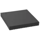
- Package: HVQFN56, SOT949-6.
- Body: 7 mm x 7 mm x 0.85 mm.
- Pitch: 0.4 mm.
- Orderable part: PCA9450CHNY, reel packing.
- Operating input range: VSYS, INL1, INB13, INB26, INB45, SWIN = 2.7 V to 5.5 V.
- Ambient temperature range: -40 °C to +105 °C.
- Junction temperature range: -40 °C to +125 °C.
- Typical thermal resistance Rth(j-a): 32.1 °C/W.
- Regulators:
- BUCK1, BUCK2, BUCK3: 0.6 V to 2.1875 V, 12.5 mV step, 3 A.
- BUCK4: 0.6 V to 3.4 V, 25 mV step, 3 A.
- BUCK5, BUCK6: 0.6 V to 3.4 V, 25 mV step, 2 A.
- PCA9450C supports BUCK1-BUCK3 as a 6 A dual-phase regulator.
- LDO1: 1.6 V to 1.9 V or 3.0 V to 3.3 V, 10 mA.
- LDO2: 0.8 V to 1.15 V, 10 mA.
- LDO3: 0.8 V to 3.3 V, 300 mA.
- LDO4: 0.8 V to 3.3 V, 200 mA.
- LDO5: 0.8 V to 3.3 V, 150 mA, selected by SD_VSEL.
- Other features: 400 mA SD-card load switch, two-channel logic level translator, 32.768 kHz crystal driver, Fm+ 1 MHz I2C, UVLO, thermal shutdown, fault monitoring.
Symbol and pin cross-check
The symbol pin numbers and names were checked against the datasheet pin description table.
Matching pins
Pins 1-29 and 30-56 are present with the expected functional names, including grouped duplicated pins:
- INB45: pins 16, 17, 18 represented as INB45_1, INB45_2, INB45_3.
- LX4: pins 19, 20 represented as LX4_1, LX4_2.
- INB13: pins 33, 34, 35 represented as INB13_1, INB13_2, INB13_3.
- LX1: pins 36, 37 represented as LX1_1, LX1_2.
- LX2: pins 45, 46 represented as LX2_1, LX2_2.
- INB26: pins 47, 48, 49 represented as INB26_1, INB26_2, INB26_3.
- LX6: pins 50, 51 represented as LX6_1, LX6_2.
Mismatches / issues flagged
- Pin 43 naming differs from datasheet:
- Project symbol: BUCK_A_GND
- Datasheet: BUCK_AGND
- Recommended action: rename to BUCK_AGND for exact datasheet consistency.
- Pin 23 naming differs from datasheet:
- Project symbol: SW_OUT
- Datasheet: SWOUT
- Recommended action: consider renaming to SWOUT, or retain SW_OUT if this is an intentional readability convention.
- Exposed pad handling:
- Datasheet package is HVQFN56 with exposed pad; EP is shown separately, not as terminal pin 57.
- Project represents EP as Pin Number 57, which is common for EDA footprints but should be documented as exposed pad rather than a numbered lead.
- Pin types and descriptions are incomplete in the project symbol:
- All terminal Pin Type properties are currently Unspecified.
- Datasheet defines P, GND, DO, DI, DIO, AI, and AO pin types.
- Recommended action: populate Pin Type and Pin Description properties for ERC accuracy and library quality.
Footprint cross-check
- Project layout contains 57 pads including EP.
- Datasheet package is HVQFN56 plus exposed pad; therefore 56 perimeter terminals + EP is expected.
- Pad count is consistent with the datasheet package concept.
- The layout tree available in this review did not expose pad dimensions, pitch, body outline, solder mask, or paste geometry; therefore geometry could not be fully verified against SOT949-6 mechanical drawings.
- Recommended action: verify footprint dimensions against datasheet Figures 26-30 / SOT949-6 land pattern: 7 mm x 7 mm body, 0.4 mm pitch, exposed pad geometry, solder mask opening, and paste stencil pattern.
Datasheet pin descriptions requiring schematic notes
- LDO4, LDO2, LDO1, LDO5: bypass each output with 1 µF to GND.
- VINT: bypass with 1 µF to GND.
- LDO3: bypass with 2.2 µF to GND.
- INL1: bypass with 4.7 µF to GND.
- VSYS: bypass with 1 µF to GND.
- INB13: bypass with two 10 µF capacitors to GND.
- INB26: bypass with 10 µF and 4.7 µF to GND.
- INB45: bypass with 10 µF and 4.7 µF to GND.
- SWIN and SWOUT: each bypass with 1 µF to GND if used.
- POR_B and IRQ_B: open-drain outputs requiring external pull-up resistors.
- SD_VSEL: must be tied high or low; do not leave floating.
- XTAL_IN: tie to GND if crystal is not used.
- XTAL_OUT: leave floating if crystal is not used.
- AGND and BUCK_AGND: connect to ground plane through vias; do not short directly to EP on the top layer.
Conclusion
The part identity, package family, target platform, symbol pin count, and footprint pad count are broadly consistent with the official NXP PCA9450 datasheet. The main library-quality issues are incomplete pin metadata, two naming inconsistencies, and the need for a mechanical land-pattern verification beyond pad count.


Welcome 👋
Flux accelerates your PCB design with AI.
Create your account to start using this component and bring your ideas to life.