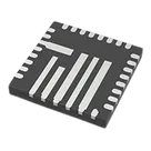
Part Information Review and Datasheet Update
Worked for 1 min 48 sec
Reviewed the parametric symbol grouping and updated the findings in MAX77961BEFV12+ Datasheet, Symbol, and Footprint Review.
Summary: the grouping is usable but not fully library-quality. Main issues:
STBY should not be in Status/Interrupt, DISQBAT should be Hardware Control, AVL/PVL should be Bias Supplies, CSINP/CSINN should be CHGIN/Input Current Sense, and BST/LX pins should be Switching Power Stage rather than generic Power Input.
Fix the symbol sections and pin groupings to match the datasheet.
Thought for 8 sec
I’ll apply the recommended datasheet-aligned section and pin group names across all 30 terminals, then verify the resulting symbol organization.
Worked for 1 min 9 sec
Fixed the parametric symbol organization across all 30 terminals.
Updated sections and pin groups now follow the datasheet functional blocks:
CHGIN / Input Current Sense, Switching Power Stage, System / Battery Power Path, Hardware Control, Charger Programming, Bias Supplies, I2C Communication, Status / Interrupt Outputs, Thermal / Battery Monitor, and Ground. Verified afterward, and the relevant terminal review checks returned no issues.Run ERC/DRC
Check I2C pullups
Review layout constraints
Document grouping
Review BOM
Name
Pin #
Type
Part Type
Pin Description
Pin Group
BST1
1
Power In
Terminal
High-side input MOSFET driver supply. Bypass BST1 to LX1 with a 0.22uF/6.3V capacitor.
Switching Power Stage
CHGIN
2
Power In
Terminal
Buck-boost charger input. CHGIN is also the buck output when operating in reverse mode. Bypass with two 10uF/35V ceramic capacitors from CHGIN to PGND.
CHGIN / Input Current Sense
LX1
3
Passive
Terminal
Inductor connection one. Connect an inductor between LX1 and LX2.
Switching Power Stage
PGND
4
Ground
Terminal
Power ground for buck-boost low-side MOSFETs.
Ground
LX2
5
Passive
Terminal
Inductor connection two. Connect an inductor between LX1 and LX2.
Switching Power Stage
SYS
6
Power Out
Terminal
System supply output. Bypass SYS to PGND with a minimum of two 47uF/25V ceramic capacitors.
System / Battery Power Path
OTGEN
7
Input
Terminal
Active-high input. Driving OTGEN high enables OTG function; when pulled low, OTG enable is controlled by I2C. Pulldown resistance must be below 44kOhm.
Hardware Control
DISQBAT
8
Input
Terminal
Active-high input. Drive high to disable the integrated QBAT FET between SYS and BATT and disable charging. Pulldown resistance must be below 44kOhm.
Hardware Control
BST2
9
Power In
Terminal
High-side output MOSFET driver supply. Bypass BST2 to LX2 with a 0.22uF/6.3V capacitor.
Switching Power Stage
BATSN
10
Input
Terminal
Battery voltage differential sense negative input. Connect to the negative terminal of the battery pack.
System / Battery Power Path
BATSP
11
Input
Terminal
Battery voltage differential sense positive input. Connect to the positive terminal of the battery pack.
System / Battery Power Path
BATT
12
Power In
Terminal
Battery power connection. Connect to the positive terminal of the battery pack. Bypass BATT to PGND with a 10uF/25V capacitor. All BATT pins must be connected together externally.
System / Battery Power Path
THM
13
Input
Terminal
Thermistor input. Connect an NTC thermistor from THM to GND and a resistor equal to the thermistor 25C resistance from THM to AVL; tie THM to GND to disable temperature sensing or to AVL to emulate battery removal.
Thermal / Battery Monitor
SCL
14
Input
Terminal
Serial interface I2C clock input.
I2C Communication
SDA
15
Bi-Directional
Terminal
Serial interface I2C data. Open-drain output.
I2C Communication
STAT
16
Output
Terminal
Charger status output. Active-low, open-drain output; connect to pullup through a 10kOhm resistor. Pulls low when charging is in progress and is high impedance otherwise.
Status / Interrupt Outputs
INOKB
17
Output
Terminal
Input Power-OK / OTG Power-OK output. Active-low, open-drain output pulls low when CHGIN voltage is valid.
Status / Interrupt Outputs
INTB
18
Output
Terminal
Active-low open-drain interrupt output. Connect a pullup resistor to the pullup power source.
Status / Interrupt Outputs
MAX77961BEFV12+