Part Review and Verification
Thought for 3 mins 58 sec
Part review result
1) Available part information
2) Datasheet property check
3) Datasheet scan summary
3b) Absolute maximum ratings recovered from official snippets
3c) Recommended operating conditions recovered
3d) Pin metadata recovered from official sources
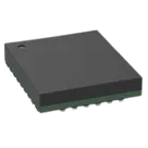
3e) Package metadata recovered
4) Cross-check: symbol and footprint vs official datasheet
Findings
My assessment
Most important risks to fix before using this part
Table
| Field | Result |
|---|---|
| Part | LT7171RV#TRMPBF |
| Description | 20 A, 16 V Silent Switcher step-down regulator with digital power system management |
| Manufacturer | Analog Devices |
| MPN | LT7171RV#TRMPBF |
| Datasheet URL property | Already set: PDF |
| Package from official sources | 30-lead LQFN, 3.5 mm x 4 mm, package drawing 05-08-7066 |
| Package in current part project | Footprint exists; schematic symbol exposes 35 numbered terminals |
| Pin numbering in current symbol | 1 to 35 |
| Nets in part project | None defined yet |
Table
| Check | Result |
|---|---|
| Datasheet URL present already? | Yes |
| Web lookup needed? | No |
| Property update needed? | No |
I attempted the full datasheet scan via
3a) Key electrical / feature metadata
@file twice, but the PDF parsing failed both times. I then fell back to official Analog Devices web results that quote the same datasheet and product page.Table
| Item | Exact value / summary |
|---|---|
| Input voltage range | 2.9 V to 16 V |
| Low input operation with EXTVCC | down to 1.5 V with EXTVCC |
| Output voltage range | 0.4 V to 5.5 V |
| Switching frequency | 400 kHz to 4 MHz |
| Output voltage accuracy | ±0.25% for 0.6 V ≤ VOUT ≤ 1.375 V |
| Architecture | Silent Switcher step-down regulator with digital power system management |
| Interface | PMBus / I2C |
| Telemetry | Readback of VOUT, IOUT, VIN, die temperature, and faults |
| Configuration | Programmable voltage, current limit, sequencing, frequency, loop compensation |
| NVM | 3-time programmable NVM |
| Sensing | Differential remote output sense |
| Multiphase | PolyPhase load sharing |
Table
| Parameter | Exact value recovered |
|---|---|
| VIN | -0.3 V to +20 V |
| EXTVCC | -0.3 V to +6 V |
| RUN / PGOOD / ALERT / SDA / SCL / SYNC / PWM_CFG / FAULT / ASEL / WP / SHARE_CLK / ITH / VOUT_CFG | -0.3 V to +6 V |
| VSENSEP | -0.3 V to +6 V |
| VSENSEN | -0.3 V to +0.3 V |
Table
| Parameter | Exact value recovered |
|---|---|
| Input voltage | 2.9 V to 16 V |
| Output voltage | 0.4 V to 5.5 V |
| Switching frequency | 400 kHz to 4 MHz |
Table
| Pin / pins | Function summary |
|---|---|
| 1, 24 | VIN power inputs |
| 2, 23, 33, 34, 35 | PGND power grounds |
| 3 | DRVCC driver supply |
| 8 | INTVCC internal bias / LDO-related supply |
| 10 | VDD18 |
| 12 | ALERT |
| 13 | RUN enable / control |
| 14 | PGOOD |
| 15 | SDA |
| 16 | SCL |
| 17 | FAULT |
| 18 | SYNC |
| 19 | SHARE_CLK |
| 20 | EXTVCC external bias supply input |
| 21 | VSENSEP positive remote sense |
| 22 | VSENSEN negative remote sense |
| 25 | BOOST1 bootstrap |
| 26, 27 | SW1 switching node |
| 28, 29 | SW0 switching node |
| 30 | BOOST0 bootstrap |
Table
| Item | Exact value recovered |
|---|---|
| Package type | 30-lead LQFN |
| Body size | 3.5 mm x 4 mm |
| Package drawing | 05-08-7066 |
| Exposed pad | Official sources indicate an exposed-pad style LQFN package |
| Full mechanical dimensions / land pattern | Not fully extracted because PDF parsing failed |
Table
| Check | Status | Why it matters |
|---|---|---|
| Pin names vs datasheet signal set | Looks consistent | The current symbol terminals align well with the official pin names recovered from the datasheet snippets. |
| Pin numbering range | Looks consistent | The current symbol uses pins 1 to 35, and official snippets confirm pins through 35 including PGND on 35. |
| Footprint exists | Yes | Good: this avoids a missing-footprint manufacturing blocker. |
| Pin electrical types in symbol | Risk | All symbol pins are currently marked Unspecified. This can weaken ERC quality and hide integration mistakes in downstream designs. |
| Package naming / pin-count metadata | High-risk mismatch to verify | Official sources say 30-lead LQFN, but the current part representation exposes 35 numbered terminals. This may be correct physically if the package naming excludes some power-style terminals or grouping conventions, but it is a red flag until the package drawing is checked directly. |
| Footprint geometry vs datasheet land pattern | Not fully verified | I could confirm pad presence only. I could not extract pad sizes, pitch, exposed-pad geometry, or courtyard from the datasheet because the PDF parsing failed. This remains the main unresolved manufacturing risk. |
Table
| Area | Verdict |
|---|---|
| Schematic symbol pin naming | Probably okay |
| Schematic symbol pin typing | Needs improvement |
| Pin count / package metadata consistency | Needs manual verification now |
| Footprint manufacturability confidence | Not yet sufficient |
Table
| Priority | Issue | Potential consequence |
|---|---|---|
| 1 | 30-lead package label vs 35-terminal implementation | Wrong package selection, wrong ordering, or incorrect footprint assumptions |
| 2 | Footprint dimensions not verified against package drawing 05-08-7066 | Assembly failure, soldering defects, exposed-pad mismatch |
| 3 | All pins typed as Unspecified | ERC misses power/control/interface mistakes |
If you want, I can continue with a stricter audit next:
- fetch review results for footprint-related issues
- inspect the footprint in more detail
- or prepare a pin-type correction table for the symbol based on the recovered pin functions
@review footprint issues
@layout inspect footprint
Pin type audit