Part Project Review Checklist
2:10
Evalu.
Using Schematic Tool.
Using BOM Tool.
Using PCB Layout Tool.
Looking for "device description, features, package options, and ordering information" in lm25117
Looking for "absolute maximum ratings" in lm25117
Looking for "recommended operating conditions" in lm25117
Looking for "electrical characteristics" in lm25117
Looking for "pin functions and terminal configuration" in lm25117
Looking for "package information and mechanical dimensions for PSQE WQFN package" in lm25117
Looking for "exposed pad, thermal pad, land pattern, and layout recommendations" in lm25117
Address.
Investig.
Assess.
Using Calculator Tool.
1) Available Project Information
| Field | Value |
|---|---|
| Project / part | This part project is for LM25117PSQE/NOPB |
| Manufacturer | Texas Instruments |
| MPN | LM25117PSQE/NOPB |
| Designator prefix | U |
| Datasheet URL present in project | Yes - PDF |
| Package in project footprint | QFN50P400X400X80-25N |
| Footprint source asset | QFN50P400X400X80-25N.kicad_mod |
| 3D model present | Yes - STEP model is attached |
| Schematic pin count | 24 terminals |
| Footprint pad count in asset | 25 pads total, including exposed pad 25 |
| Project description | LM25117PSQE/NOPB RTW24_2P6X2P6_TEX RTW24_2P6X2P6_TEX-M RTW24_2P6X2P6_TEX-L |
2) Datasheet Status
| Check | Result |
|---|---|
| Datasheet already set? | Yes |
| Web search needed? | No |
| Property update needed? | No |
Device Overview and Special Features
| Category | Summary |
|---|---|
| Function | Synchronous buck controller for high-voltage / wide-input step-down regulators |
| Control method | Emulated peak current mode control |
| Input operating range | 4.5 V to 42 V |
| Frequency range | Programmable from 50 kHz to 750 kHz |
| Output programming | Programmable output from 0.8 V reference |
| Gate drive | External high-side and low-side NMOS gate drivers, adaptive dead-time control |
| Notable features | Diode emulation mode, analog current monitor, programmable current limit, hiccup overcurrent protection, soft-start/tracking, programmable UVLO, thermal shutdown |
| Internal bias behavior | Internal high-voltage bias regulator, with optional switchover to external bias supply |
Ordering / Package Metadata
| Item | Datasheet Value |
|---|---|
| Exact orderable | LM25117PSQE/NOPB |
| Package family | WQFN (RTW) |
| Pin count | 24 pins |
| Body size | 4.00 mm x 4.00 mm |
| Max package height | 0.8 mm max |
| MSL | Level-1-260C-UNLIM |
| Part marking | L25117P |
Absolute Maximum Ratings
| Parameter | Min | Max | Unit |
|---|---|---|---|
| VIN to AGND | -0.3 | 45 | V |
| SW to AGND | -3.0 | 45 | V |
| HB to SW | -0.3 | 15 | V |
| VCC to AGND | -0.3 | 15 | V |
| HO to SW | -0.3 | HB + 0.3 | V |
| LO to AGND | -0.3 | VCC + 0.3 | V |
| FB, DEMB, RES, VCCDIS, UVLO to AGND | -0.3 | 15 | V |
| CM, COMP to AGND | -0.3 | 7 | V |
| SS, RAMP, RT to AGND | -0.3 | 7 | V |
| CS, CSG, PGND to AGND | -0.3 | 0.3 | V |
| Storage temperature | -55 | 150 | °C |
| Junction temperature | -40 | 150 | °C |
Recommended Operating Conditions
| Parameter | Min | Max | Unit |
|---|---|---|---|
| VIN | 4.5 | 42 | V |
| VCC | 4.5 | 14 | V |
| HB to SW | 4.5 | 14 | V |
| Junction temperature | -40 | 125 | °C |
Key Electrical Characteristics
| Category | Parameter | Min | Typ | Max | Unit |
|---|---|---|---|---|---|
| VIN supply | Operating current | - | 4.8 | 6.2 | mA |
| VIN supply | Shutdown current | - | 16 | 40 | µA |
| VCC regulator | Regulation | 6.85 | 7.6 | 8.2 | V |
| VCC regulator | Sourcing current limit | - | 30 | 42 | mA |
| VCC UVLO | Rising threshold | 3.75 | 4.0 | 4.15 | V |
| VCCDIS | Rising threshold | 1.22 | 1.25 | 1.29 | V |
| UVLO | Rising threshold | 1.22 | 1.25 | 1.29 | V |
| Soft-start | SS current source | 7 | 10 | 12 | µA |
| Feedback | FB reference voltage | 788 | 800 | 812 | mV |
| Error amp | DC gain | - | 80 | - | dB |
| Error amp | Unity gain bandwidth | - | 3 | - | MHz |
| Oscillator | RT = 25 kOhm | 180 | 200 | 220 | kHz |
| Oscillator | RT = 10 kOhm | 430 | 480 | 530 | kHz |
| Current limit | Sense threshold | 106 | 120 | 135 | mV |
| HO driver | Peak source current | - | 2.2 | - | A |
| HO driver | Peak sink current | - | 3.3 | - | A |
| LO driver | Peak source current | - | 2.5 | - | A |
| LO driver | Peak sink current | - | 3.3 | - | A |
| Thermal | Shutdown | - | 165 | - | °C |
Pin Descriptions
| WQFN Pin | Name | Datasheet Type | Datasheet Description |
|---|---|---|---|
| 1 | DEMB | Input | Enables diode emulation when low; internal 50 kOhm pull-down |
| 2 | RES | Output | Restart timer for hiccup mode using external capacitor |
| 3 | SS | Input | Soft-start ramp capacitor input with internal 10 µA source |
| 4 | RT | Input | Oscillator programming / sync input |
| 5 | AGND | Ground | Analog ground |
| 6 | NC | NC | No electrical contact |
| 7 | VCCDIS | Input | Disables internal VCC regulator when above 1.25 V |
| 8 | FB | Input | Feedback input, regulation threshold 0.8 V |
| 9 | COMP | Output | Error amplifier output |
| 10 | CM | Output | Average sensed inductor current monitor |
| 11 | RAMP | Input | PWM ramp signal input |
| 12 | CS | Input | Current sense input, high side of sense resistor |
| 13 | CSG | Input | Kelvin ground sense to current sense resistor |
| 14 | PGND | Ground | Power ground return for low-side gate driver |
| 15 | LO | Output | Low-side NMOS gate drive |
| 16 | VCC | Power / Output / Input | Bias supply pin, decouple locally to PGND |
| 17 | NC | NC | No electrical contact |
| 18 | SW | Input / Output | Switching node |
| 19 | HO | Output | High-side NMOS gate drive |
| 20 | HB | Power | Bootstrap supply |
| 21 | NC | NC | No electrical contact |
| 22 | VIN | Power / Input | Supply input for VCC regulator |
| 23 | NC | NC | No electrical contact |
| 24 | UVLO | Input | Undervoltage lockout programming pin |
| 25 | EP | Exposed pad | Electrically isolated; should be soldered to ground plane for thermal performance |
Package Dimensions and Land Pattern
| Item | Datasheet Value |
|---|---|
| Package code | RTW0024A |
| Package type | WQFN |
| Package size A | 4.1 / 3.9 mm |
| Package size B | 4.1 / 3.9 mm |
| Lead pitch | 0.5 mm |
| Lead width | 0.3 / 0.2 mm |
| Lead length | 0.5 / 0.3 mm |
| Exposed pad | 2.6 mm +/- 0.1 mm square |
| Board-layout terminal pad example | 24x (0.25 mm x 0.6 mm) |
| Pad clearance around body | 0.07 mm min / 0.07 mm max all around |
| Stencil guidance | 78% printed solder coverage on exposed pad |
| Mask style | Non-solder-mask-defined preferred |
Cross-Check Findings
| Area | Result | Risk | Details |
|---|---|---|---|
| MPN vs package | Pass | Low | Project MPN and datasheet orderable both match LM25117PSQE/NOPB, which is the 24-pin RTW WQFN version. |
| Symbol pin count vs datasheet | Pass | Low | Symbol has 24 terminals, matching the package pin count. |
| Footprint package family | Pass | Low | Footprint asset name indicates 4.0 mm x 4.0 mm, 0.5 mm pitch, 25-pad QFN, consistent with datasheet package family. |
| Exposed pad presence | Partial pass | Medium | Footprint asset includes pad 25 at 2.6 mm x 2.6 mm, matching datasheet EP size. |
| Exposed pad in symbol | Needs review | Medium | The symbol exposes only 24 terminals and does not include an EP terminal. Since the datasheet says EP is electrically isolated, that is electrically acceptable, but the package note still requires it to be soldered for thermal/mechanical performance. |
| Exposed pad soldering guidance | Concern | High | Datasheet says EP should be soldered to the ground plane and is critical for thermal/mechanical performance. If this footprint instance does not preserve pad 25 and its paste/mask correctly in manufacturing output, assembly reliability can suffer. |
| Perimeter pad size | Deviation | Medium | Datasheet example land pattern is 0.25 mm x 0.6 mm. Imported footprint pads appear to be about 0.27 mm x 0.86 mm. That is noticeably longer than TI's example and should be verified against the intended IPC or source-library footprint. |
| EP stencil coverage | Mismatch | High | Datasheet calls for 78% solder coverage under EP. The footprint asset appears to define a single paste opening about 1.64 mm x 1.64 mm, which is only about 39.8% of EP area. That is a significant mismatch. |
| Pin naming consistency | Pass | Low | Symbol terminal names line up with datasheet names and pin numbers. |
| Pin type metadata | Mismatch | Low to Medium | Several pin electrical types in the symbol metadata do not match datasheet function. This usually will not break manufacturing, but can weaken ERC quality and part correctness. |
| No-connect pins | Pass | Low | NC pins are present in symbol and footprint positions consistent with datasheet. |
Pin-Type Metadata Mismatches
| Pin | Datasheet Role | Current Project Role | Impact |
|---|---|---|---|
| VIN, pin 22 | Power / Input | Input | ERC quality issue |
| UVLO, pin 24 | Input | Unspecified | ERC quality issue |
| RES, pin 2 | Output | Unspecified | ERC quality issue |
| HB, pin 20 | Power | Unspecified | ERC quality issue |
| SW, pin 18 | Input / Output | Unspecified | ERC quality issue |
| CSG, pin 13 | Input | Unspecified | ERC quality issue |
| AGND, pin 5 | Ground | Power In | ERC semantics issue |
| PGND, pin 14 | Ground | Power In | ERC semantics issue |
| VCC, pin 16 | Power / Output / Input | Power In | Slight semantic mismatch |
| RAMP, pin 11 | Input | Unspecified | ERC quality issue |
Bottom Line
| Severity | Finding |
|---|---|
| High | The exposed-pad stencil definition appears inconsistent with the datasheet's 78% paste recommendation. |
| High | The thermal / mechanical exposed-pad implementation must be verified in final manufacturing outputs. |
| Medium | The perimeter copper pad size deviates from TI's example board layout and should be confirmed against the intended footprint source. |
| Low / Medium | Several symbol pin types should be corrected to improve rule checking and part accuracy. |
Recommended Fixes
| Priority | Action |
|---|---|
| 1 | Verify that exposed pad 25 is truly present in the generated footprint/manufacturing outputs and not lost due to missing symbol mapping. |
| 2 | Adjust the exposed-pad paste pattern to match TI's stencil guidance much more closely. |
| 3 | Recheck perimeter pad dimensions against TI's RTW example land pattern or the exact source-library recommendation used to generate this footprint. |
| 4 | Correct symbol electrical pin types for VIN, UVLO, RES, HB, SW, CSG, AGND, PGND, VCC, and RAMP. |
Ready.
Reviews

- Wirelessly connects nets on schematic. Used to organize schematics and separate functional blocks. To wirelessly connect net portals, give them same designator. #portaljharwinbarrozo43.0M
- Wirelessly connects power nets on schematic. Identical to the net portal, but with a power symbol. Used to organize schematics and separate functional blocks. To wirelessly connect power net portals, give them the same designator. #portal #powerjharwinbarrozo11.4M
- A generic fixed resistor for rapid developing circuit topology. Save precious design time by seamlessly add more information to this part (value, footprint, etc.) as it becomes available. Standard resistor values: 1.0Ω 10Ω 100Ω 1.0kΩ 10kΩ 100kΩ 1.0MΩ 1.1Ω 11Ω 110Ω 1.1kΩ 11kΩ 110kΩ 1.1MΩ 1.2Ω 12Ω 120Ω 1.2kΩ 12kΩ 120kΩ 1.2MΩ 1.3Ω 13Ω 130Ω 1.3kΩ 13kΩ 130kΩ 1.3MΩ 1.5Ω 15Ω 150Ω 1.5kΩ 15kΩ 150kΩ 1.5MΩ 1.6Ω 16Ω 160Ω 1.6kΩ 16kΩ 160kΩ 1.6MΩ 1.8Ω 18Ω 180Ω 1.8KΩ 18kΩ 180kΩ 1.8MΩ 2.0Ω 20Ω 200Ω 2.0kΩ 20kΩ 200kΩ 2.0MΩ 2.2Ω 22Ω 220Ω 2.2kΩ 22kΩ 220kΩ 2.2MΩ 2.4Ω 24Ω 240Ω 2.4kΩ 24kΩ 240kΩ 2.4MΩ 2.7Ω 27Ω 270Ω 2.7kΩ 27kΩ 270kΩ 2.7MΩ 3.0Ω 30Ω 300Ω 3.0KΩ 30KΩ 300KΩ 3.0MΩ 3.3Ω 33Ω 330Ω 3.3kΩ 33kΩ 330kΩ 3.3MΩ 3.6Ω 36Ω 360Ω 3.6kΩ 36kΩ 360kΩ 3.6MΩ 3.9Ω 39Ω 390Ω 3.9kΩ 39kΩ 390kΩ 3.9MΩ 4.3Ω 43Ω 430Ω 4.3kΩ 43KΩ 430KΩ 4.3MΩ 4.7Ω 47Ω 470Ω 4.7kΩ 47kΩ 470kΩ 4.7MΩ 5.1Ω 51Ω 510Ω 5.1kΩ 51kΩ 510kΩ 5.1MΩ 5.6Ω 56Ω 560Ω 5.6kΩ 56kΩ 560kΩ 5.6MΩ 6.2Ω 62Ω 620Ω 6.2kΩ 62KΩ 620KΩ 6.2MΩ 6.8Ω 68Ω 680Ω 6.8kΩ 68kΩ 680kΩ 6.8MΩ 7.5Ω 75Ω 750Ω 7.5kΩ 75kΩ 750kΩ 7.5MΩ 8.2Ω 82Ω 820Ω 8.2kΩ 82kΩ 820kΩ 8.2MΩ 9.1Ω 91Ω 910Ω 9.1kΩ 91kΩ 910kΩ 9.1MΩ #generics #CommonPartsLibraryjharwinbarrozo1.5M
- A generic fixed capacitor ideal for rapid circuit topology development. You can choose between polarized and non-polarized types, its symbol and the footprint will automatically adapt based on your selection. Supported options include standard SMD sizes for ceramic capacitors (e.g., 0402, 0603, 0805), SMD sizes for aluminum electrolytic capacitors, and through-hole footprints for polarized capacitors. Save precious design time by seamlessly add more information to this part (value, footprint, etc.) as it becomes available. Standard capacitor values: 1.0pF 10pF 100pF 1000pF 0.01uF 0.1uF 1.0uF 10uF 100uF 1000uF 10,000uF 1.1pF 11pF 110pF 1100pF 1.2pF 12pF 120pF 1200pF 1.3pF 13pF 130pF 1300pF 1.5pF 15pF 150pF 1500pF 0.015uF 0.15uF 1.5uF 15uF 150uF 1500uF 1.6pF 16pF 160pF 1600pF 1.8pF 18pF 180pF 1800pF 2.0pF 20pF 200pF 2000pF 2.2pF 22pF 20pF 2200pF 0.022uF 0.22uF 2.2uF 22uF 220uF 2200uF 2.4pF 24pF 240pF 2400pF 2.7pF 27pF 270pF 2700pF 3.0pF 30pF 300pF 3000pF 3.3pF 33pF 330pF 3300pF 0.033uF 0.33uF 3.3uF 33uF 330uF 3300uF 3.6pF 36pF 360pF 3600pF 3.9pF 39pF 390pF 3900pF 4.3pF 43pF 430pF 4300pF 4.7pF 47pF 470pF 4700pF 0.047uF 0.47uF 4.7uF 47uF 470uF 4700uF 5.1pF 51pF 510pF 5100pF 5.6pF 56pF 560pF 5600pF 6.2pF 62pF 620pF 6200pF 6.8pF 68pF 680pF 6800pF 0.068uF 0.68uF 6.8uF 68uF 680uF 6800uF 7.5pF 75pF 750pF 7500pF 8.2pF 82pF 820pF 8200pF 9.1pF 91pF 910pF 9100pF #generics #CommonPartsLibraryjharwinbarrozo1.5M
- A generic fixed inductor for rapid developing circuit topology. *You can now change the footprint and 3D model at the top level anytime you want. This is the power of #genericsjharwinbarrozo15.5k
- An electrical connector acting as reusable interface to a conductor and creating a point where external circuits can be connected.Terminal
- 47 kOhms ±5% 0.125W, 1/8W Chip Resistor 0805 (2012 Metric) Automotive AEC-Q200 Thick Film #forLedBlinkjharwinbarrozo1.2M
- 10uF Capacitor Aluminum Polymer 20% 16V SMD 5x5.3mm #forLedBlink #commonpartslibrary #capacitor #aluminumpolymer #radialcanjharwinbarrozo1.2M
- Yellow 595nm LED Indication - Discrete 1.7V 1206 (3216 Metric) #forLedBlinkjharwinbarrozo1.1M


Pricing & Availability
See prices from popular manufacturers for your project.
Assets

LM25117PSQE_NOPB
LM25117PSQE_NOPB LM25117PSQE_NOPB_0_1 Symbol.svgDefaultLM25117PSQE_NOPB
LM25117PSQE_NOPB.step3D Model
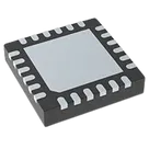
LM25117PSQENOPB-thumb.png
LM25117PSQENOPB-thumbThumbnailLM25117PSQE_NOPB
QFN50P400X400X80-25N.kicad_modFootprintControls
Welcome 👋
Flux accelerates your PCB design with AI.
Create your account to start using this component and bring your ideas to life.