Part Datasheet Review and Verification
4:15
Review.
Extract.
Using Schematic Tool.
Looking for "part description and key features" in da2032.pdf
Looking for "applications or intended controller reference (e.g., LT3750)" in da2032.pdf
Looking for "electrical characteristics table" in da2032.pdf
Looking for "absolute maximum ratings" in da2032.pdf
Looking for "recommended operating conditions" in da2032.pdf
Looking for "pinout or pin descriptions, primary and secondary pin numbers" in da2032.pdf
Looking for "turns ratio, inductance, leakage inductance, DCR primary and secondary" in da2032.pdf
Looking for "isolation voltage or hipot rating" in da2032.pdf
Looking for "saturation current or current ratings" in da2032.pdf
Looking for "package dimensions mechanical drawing" in da2032.pdf
Looking for "recommended land pattern or pad layout" in da2032.pdf
Looking for "operating temperature range and storage temperature" in da2032.pdf
Looking for "notes about polarity dots and pin numbering" in da2032.pdf
Using PCB Layout Tool.
Using PCB Layout Tool.
Looking for "pin numbering diagram showing which pins are primary and which are secondary for DA2032-AL" in da2032.pdf
Looking for "text identifying which specific pin numbers belong to primary windings and which to secondary for DA2032-AL" in da2032.pdf
Looking for "note: Primary windings to be connected in parallel on PC board - identify which pins connect together" in da2032.pdf
Looking for "Which pin numbers are secondary for DA2032-AL" in da2032.pdf
Looking for "Which pin numbers are primary for DA2032-AL" in da2032.pdf
Looking for "diagram labels Primary and Secondary next to pin numbers list" in da2032.pdf
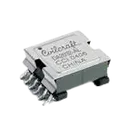
- MPN: DA2032-ALD
- Manufacturer: COILCRAFT
- Part Type: Transformers
- Mount: Surface Mount
- Package/Case Code: SMD
- Description: COILCRAFT - DA2032-ALD - TRANSFORMER, FLYBACK, LT3750, SMD
- Datasheet: https://www.coilcraft.com/pdfs/da2032.pdf
- Pin count (from schematic symbol): 12 terminals
- SECONDARY_1 — Pin Number: 1
- PRIMARY_1 — Pin Number: 2
- PRIMARY_2 — Pin Number: 3
- PRIMARY_3 — Pin Number: 4
- PRIMARY_4 — Pin Number: 5
- PRIMARY_5 — Pin Number: 6
- PRIMARY_6 — Pin Number: 7
- PRIMARY_7 — Pin Number: 8
- PRIMARY_8 — Pin Number: 9
- PRIMARY_9 — Pin Number: 10
- PRIMARY_10 — Pin Number: 11
- SECONDARY_2 — Pin Number: 12
- Pads found: SECONDARY_1, PRIMARY_1..PRIMARY_10, SECONDARY_2 (12 total)
- A datasheet URL is already set for this part (https://www.coilcraft.com/pdfs/da2032.pdf). No changes were needed.
- Flyback transformer for Linear Technology LT3750/LT3751 capacitor charger controllers; designed for 3–24 V input and charging to 300 V.
- Low-profile, surface mount; smaller footprint for this application.
- Isolation: 1500 Vrms, 1 minute winding-to-winding; 750 Vrms winding-to-core.
- MSL: 1; RoHS compliant terminations.
- Primary inductance: 10.0 µH ±10% at 0 A
- Minimum inductance at Ipk: 9.0 µH
- Peak primary current (Ipk): 3.0 A
- DCR max: primary 0.013 Ω; secondary 1.60 Ω
- Leakage inductance max: 0.150 µH
- Interwinding capacitance: 67 pF
- Turns ratio (pri:sec): 1:10
- Winding-to-winding isolation: 1500 Vrms, 1 minute
- Winding-to-core isolation: 750 Vrms
- Ambient temperature: −40°C to +125°C
- Storage temperature: component −40°C to +125°C; tape & reel −40°C to +80°C
- Solder reflow: Max three 40 s reflows at +260°C (cool to room temp between cycles)
- MSL: 1 (unlimited floor life at <30°C / 85% RH)
- Intended with LT3750 (DA2032: 300 V, 3 A charge circuit example); input range 3–24 V; capacitor charge target 300 V.
- Electrical specifications provided at 25°C.
- 12-pin package with a pin 1 polarity dot indicated on the mechanical drawing.
- Note: “Primary windings to be connected in parallel on PC board.”
- Measurement notes:
- Capacitance measured at 100 kHz, 0.1 Vrms from pin 3 to pin 1 with all other pins shorted.
- DCR and leakage inductance specified with primary windings connected in parallel (and secondary shorted for leakage).
- Body length: 0.865 in (21.97 mm)
- Body width: 0.590 in (14.98 mm)
- Body height: 0.098 in (2.50 mm) max
- Additional callouts in drawing include: 0.135 in (3.43 mm), 0.070 in (1.79 mm), 0.350 in (8.89 mm), 0.079 in (2.01 mm), 0.677 in (17.20 mm), 0.693 in (17.60 mm), 0.665 in (16.88 mm), 0.028 in (0.72 mm), 0.004 in (0.10 mm)
- Dot indicates pin 1; “1–12, 6–7 pin orientation shown.”
- Drawing provided in datasheet with these pad dimension callouts:
- 0.070 in (1.79 mm)
- 0.130 in (3.30 mm)
- 0.028 in (0.711 mm)
- 0.100 in (2.54 mm)
- 0.100 in (2.54 mm)
- Pin 1 indicator is called out in the land pattern (“Dot indicates pin 1”).
- Designed specifically for LT3750-based capacitor charger (DA2032 = 300 V, 3 A example circuit).
- Two primary windings intended to be paralleled on the PCB per datasheet guidance.
- Pin count: 12 in the schematic symbol and 12 pads in the footprint — matches the datasheet’s 12-pin package.
- Numeric pin indexing: The symbol terminals have explicit Pin Number properties 1–12, which is required to align with datasheet numbering.
- Symbol-to-footprint naming: Footprint pads share the same names as symbol terminals (PRIMARY_x, SECONDARY_x), ensuring logical name matching between symbol and footprint.
- Pin role mapping (primary vs secondary):
- The symbol labels Pin 1 as SECONDARY_1 and Pin 12 as SECONDARY_2.
- The datasheet’s pinout diagram shows which numbered pins belong to the primary vs secondary windings, and includes instructions to parallel the primary windings. Because the PDF’s pinout diagram is graphical, text extraction is ambiguous. Please visually confirm that the roles associated with numeric pins 1–12 in your symbol match the datasheet’s diagram before production. If they don’t, rename the affected symbol pins to prevent wiring mistakes.
- Primary windings parallel requirement:
- The datasheet requires the primary windings to be connected in parallel on the PCB. Ensure your schematic usage notes or reference design clearly state which primary pins are to be paralleled, matching the datasheet diagram. Right now, the part project has no nets (expected), so this is a documentation/checklist item for downstream designs.
- Pin 1 indicator on footprint:
- The datasheet shows a dot for pin 1 on both the package drawing and land pattern. The current layout listing doesn’t expose silkscreen graphics; verify the footprint includes a clear pin 1 marker (silkscreen or copper chamfer) aligned with the datasheet orientation.
- Land pattern dimensions:
- The footprint node list confirms 12 pads, but the geometric details were not exposed via the layout query. Compare your pad sizes and row/column spacing to the datasheet’s recommended land pattern (e.g., 2.54 mm pitch callouts, pad widths of 0.028 in, etc.). Any deviation here can cause soldering or fit issues.
- Clearance/isolation considerations:
- With 1500 Vrms winding-to-winding isolation, ensure the footprint maintains adequate creepage/clearance between primary and secondary pad groups per your assembly voltage environment. The datasheet drawing dimensions help validate pad-row spacing; verify your footprint geometry aligns.
- No hard mismatches were found for pin count or the presence of numbered pins.
- Two critical items need human visual confirmation against the datasheet figure: which numeric pins are primary vs secondary (and correct parallel connections), and that the footprint’s land pattern and pin 1 marker match the datasheet’s recommended drawing.
- Once these are confirmed or adjusted, the part should be safe for use with LT3750-based capacitor charger designs as intended.
Ready.
Reviews

- Wirelessly connects nets on schematic. Used to organize schematics and separate functional blocks. To wirelessly connect net portals, give them same designator. #portaljharwinbarrozo43.0M
- Wirelessly connects power nets on schematic. Identical to the net portal, but with a power symbol. Used to organize schematics and separate functional blocks. To wirelessly connect power net portals, give them the same designator. #portal #powerjharwinbarrozo11.4M
- A generic fixed resistor for rapid developing circuit topology. Save precious design time by seamlessly add more information to this part (value, footprint, etc.) as it becomes available. Standard resistor values: 1.0Ω 10Ω 100Ω 1.0kΩ 10kΩ 100kΩ 1.0MΩ 1.1Ω 11Ω 110Ω 1.1kΩ 11kΩ 110kΩ 1.1MΩ 1.2Ω 12Ω 120Ω 1.2kΩ 12kΩ 120kΩ 1.2MΩ 1.3Ω 13Ω 130Ω 1.3kΩ 13kΩ 130kΩ 1.3MΩ 1.5Ω 15Ω 150Ω 1.5kΩ 15kΩ 150kΩ 1.5MΩ 1.6Ω 16Ω 160Ω 1.6kΩ 16kΩ 160kΩ 1.6MΩ 1.8Ω 18Ω 180Ω 1.8KΩ 18kΩ 180kΩ 1.8MΩ 2.0Ω 20Ω 200Ω 2.0kΩ 20kΩ 200kΩ 2.0MΩ 2.2Ω 22Ω 220Ω 2.2kΩ 22kΩ 220kΩ 2.2MΩ 2.4Ω 24Ω 240Ω 2.4kΩ 24kΩ 240kΩ 2.4MΩ 2.7Ω 27Ω 270Ω 2.7kΩ 27kΩ 270kΩ 2.7MΩ 3.0Ω 30Ω 300Ω 3.0KΩ 30KΩ 300KΩ 3.0MΩ 3.3Ω 33Ω 330Ω 3.3kΩ 33kΩ 330kΩ 3.3MΩ 3.6Ω 36Ω 360Ω 3.6kΩ 36kΩ 360kΩ 3.6MΩ 3.9Ω 39Ω 390Ω 3.9kΩ 39kΩ 390kΩ 3.9MΩ 4.3Ω 43Ω 430Ω 4.3kΩ 43KΩ 430KΩ 4.3MΩ 4.7Ω 47Ω 470Ω 4.7kΩ 47kΩ 470kΩ 4.7MΩ 5.1Ω 51Ω 510Ω 5.1kΩ 51kΩ 510kΩ 5.1MΩ 5.6Ω 56Ω 560Ω 5.6kΩ 56kΩ 560kΩ 5.6MΩ 6.2Ω 62Ω 620Ω 6.2kΩ 62KΩ 620KΩ 6.2MΩ 6.8Ω 68Ω 680Ω 6.8kΩ 68kΩ 680kΩ 6.8MΩ 7.5Ω 75Ω 750Ω 7.5kΩ 75kΩ 750kΩ 7.5MΩ 8.2Ω 82Ω 820Ω 8.2kΩ 82kΩ 820kΩ 8.2MΩ 9.1Ω 91Ω 910Ω 9.1kΩ 91kΩ 910kΩ 9.1MΩ #generics #CommonPartsLibraryjharwinbarrozo1.5M
- A generic fixed capacitor ideal for rapid circuit topology development. You can choose between polarized and non-polarized types, its symbol and the footprint will automatically adapt based on your selection. Supported options include standard SMD sizes for ceramic capacitors (e.g., 0402, 0603, 0805), SMD sizes for aluminum electrolytic capacitors, and through-hole footprints for polarized capacitors. Save precious design time by seamlessly add more information to this part (value, footprint, etc.) as it becomes available. Standard capacitor values: 1.0pF 10pF 100pF 1000pF 0.01uF 0.1uF 1.0uF 10uF 100uF 1000uF 10,000uF 1.1pF 11pF 110pF 1100pF 1.2pF 12pF 120pF 1200pF 1.3pF 13pF 130pF 1300pF 1.5pF 15pF 150pF 1500pF 0.015uF 0.15uF 1.5uF 15uF 150uF 1500uF 1.6pF 16pF 160pF 1600pF 1.8pF 18pF 180pF 1800pF 2.0pF 20pF 200pF 2000pF 2.2pF 22pF 20pF 2200pF 0.022uF 0.22uF 2.2uF 22uF 220uF 2200uF 2.4pF 24pF 240pF 2400pF 2.7pF 27pF 270pF 2700pF 3.0pF 30pF 300pF 3000pF 3.3pF 33pF 330pF 3300pF 0.033uF 0.33uF 3.3uF 33uF 330uF 3300uF 3.6pF 36pF 360pF 3600pF 3.9pF 39pF 390pF 3900pF 4.3pF 43pF 430pF 4300pF 4.7pF 47pF 470pF 4700pF 0.047uF 0.47uF 4.7uF 47uF 470uF 4700uF 5.1pF 51pF 510pF 5100pF 5.6pF 56pF 560pF 5600pF 6.2pF 62pF 620pF 6200pF 6.8pF 68pF 680pF 6800pF 0.068uF 0.68uF 6.8uF 68uF 680uF 6800uF 7.5pF 75pF 750pF 7500pF 8.2pF 82pF 820pF 8200pF 9.1pF 91pF 910pF 9100pF #generics #CommonPartsLibraryjharwinbarrozo1.5M
- A generic fixed inductor for rapid developing circuit topology. *You can now change the footprint and 3D model at the top level anytime you want. This is the power of #genericsjharwinbarrozo15.5k
- An electrical connector acting as reusable interface to a conductor and creating a point where external circuits can be connected.Terminal
- 47 kOhms ±5% 0.125W, 1/8W Chip Resistor 0805 (2012 Metric) Automotive AEC-Q200 Thick Film #forLedBlinkjharwinbarrozo1.2M
- 10uF Capacitor Aluminum Polymer 20% 16V SMD 5x5.3mm #forLedBlink #commonpartslibrary #capacitor #aluminumpolymer #radialcanjharwinbarrozo1.2M
- Yellow 595nm LED Indication - Discrete 1.7V 1206 (3216 Metric) #forLedBlinkjharwinbarrozo1.1M


Pricing & Availability
See prices from popular manufacturers for your project.
Assets
DA2032-ALD
DA2032-ALD.stp3D Model
DA2032-ALD-thumb.png
DA2032-ALD-thumbThumbnailDA2032-ALD
SOP250P2197X889-12N.kicad_modFootprint
DA2032-ALD
DA2032-ALD Symbol.svgDefaultControls
Welcome 👋
Flux accelerates your PCB design with AI.
Create your account to start using this component and bring your ideas to life.