Part Project Execution Steps
5:38
Evalu.
Analy.
Checking.
Analyzing the schematic.
Analyzing the PCB layout.
Reviewing the bill of materials.
Looking for "Features list" in avagotechnologies_ADNS-3050-1217285.pdf
Looking for "Pin description table" in avagotechnologies_ADNS-3050-1217285.pdf
Looking for "Pinout diagram or pin configuration" in avagotechnologies_ADNS-3050-1217285.pdf
Looking for "Package dimensions mechanical outline" in avagotechnologies_ADNS-3050-1217285.pdf
Looking for "Absolute Maximum Ratings" in avagotechnologies_ADNS-3050-1217285.pdf
Looking for "Recommended Operating Conditions" in avagotechnologies_ADNS-3050-1217285.pdf
Looking for "Electrical Characteristics table" in avagotechnologies_ADNS-3050-1217285.pdf
Looking for "Supply voltage VDD and VIO levels" in avagotechnologies_ADNS-3050-1217285.pdf
Looking for "Current consumption or supply current" in avagotechnologies_ADNS-3050-1217285.pdf
Looking for "Resolution counts per inch (CPI or DPI)" in avagotechnologies_ADNS-3050-1217285.pdf
Looking for "Maximum speed (inches per second) and acceleration (g)" in avagotechnologies_ADNS-3050-1217285.pdf
Looking for "Frame rate or image acquisition rate" in avagotechnologies_ADNS-3050-1217285.pdf
Looking for "Image array size or pixel resolution" in avagotechnologies_ADNS-3050-1217285.pdf
Looking for "Serial interface type and timing (SPI)" in avagotechnologies_ADNS-3050-1217285.pdf
Looking for "LED illumination or wavelength and drive" in avagotechnologies_ADNS-3050-1217285.pdf
Looking for "Operating temperature range" in avagotechnologies_ADNS-3050-1217285.pdf
Looking for "Package outline dimensions numeric values mm for 8-pin DIP package of ADNS-3050" in avagotechnologies_ADNS-3050-1217285.pdf
Looking for "Recommended PCB mechanical cutouts dimensions and spacing numeric values" in avagotechnologies_ADNS-3050-1217285.pdf
Looking for "Pin pitch and row spacing for 8-pin DIP package" in avagotechnologies_ADNS-3050-1217285.pdf
Analyzing the PCB layout.
- Review of currently available part information
- MPN: ADNS-3050
- Manufacturer: Avago Technologies
- Part type: Sensors
- Designator prefix: IC
- Datasheet: PDF
- Schematic symbol status:
- Footprint status:
- Present: df3f2e1e-4727-4f32-990a-225f579bf849.defaultFootprint
- Source asset: ADNS3050.kicad_mod
- Through-hole pads (drill 0.8 mm, pad dia 1.3 mm), staggered DIP pattern (pads 1–4 along one edge, 5–8 along opposite edge)
- 3D model referenced: ADNS-3050.stp
- Datasheet presence check
- A datasheet URL is already set: PDF
- No changes required.
- Datasheet scan — extracted and summarized metadata Features
- Small Form Factor Package - 8-pin DIP
- Operating voltage: 2.8 V to 3.0 V
- High-speed motion: 60 ips (typ), acceleration up to 20 g
- Selectable resolutions up to 2000 cpi
- Four-wire SPI serial interface
- External MOTION interrupt (active low)
- Internal oscillator (no external clock)
- On-chip LED driver with configurable modes and drive current
- Programmable power-saving/rest modes
- Supports LED auto-current control; recommended red LED HLMP-EG3E; not designed for blue LED
Table
| Pin | Name | Type | Description |
|---|---|---|---|
| 1 | MISO | Output | Serial Data Output (Master In/Slave Out) |
| 2 | LED | Input | LED Illumination Control Input |
| 3 | MOTION | Output | Motion Interrupt Output (Active low) |
| 4 | NCS | Input | Chip Select (Active low) |
| 5 | SCLK | Input | Serial Clock Input |
| 6 | GND | Ground | Ground |
| 7 | VDD | Power | Supply Voltage |
| 8 | MOSI | Input | Serial Data Input (Master Out/Slave In) |
Table
| Parameter | Symbol | Min | Max | Units | Notes |
|---|---|---|---|---|---|
| Storage Temperature | TS | -40 | 85 | °C | |
| Operating Temperature | TA | -15 | 55 | °C | |
| Lead Solder Temperature | TSOLDER | 260 | °C | 7 s, 1.6 mm below seating plane | |
| Supply Voltage | VDD | -0.5 | 3.7 | V | |
| ESD (HBM) | 2 | kV | All pins | ||
| Input Voltage | VIN | -0.5 | VDD + 0.5 | V | All I/O pins |
| Output Current | Iout | 7 | mA | MISO pin |
Table
| Parameter | Symbol | Min | Typ | Max | Units | Notes |
|---|---|---|---|---|---|---|
| Operating Temperature | TA | 0 | 40 | °C | ||
| Power Supply Voltage | VDD | 2.8 | 3.0 | V | ||
| Power Supply Rise Time | tRT | 0.005 | 100 | ms | 0 to VDD min | |
| Supply Noise (Sinusoidal) | VNA | 100 | mVp-p | 10 kHz–50 MHz | ||
| Serial Port Clock Frequency | fSCLK | 1 | MHz | 50% duty | ||
| Distance Lens-to-Surface | Z | 2.3 | 2.4 | 2.5 | mm | |
| Speed | S | 60 | ips | |||
| Acceleration | A | 20 | g | In run mode | ||
| Load Capacitance (MISO) | Cout | 100 | pF |
Table
| Parameter | Symbol | Min | Typ | Max | Units | Notes |
|---|---|---|---|---|---|---|
| DC Supply Current (Run, DC) | IDD_RUN_DC | 26.604 | mA | Includes LED current; no load on MISO | ||
| DC Supply Current (Run, Wireless) | IDD_RUN_WIRELESS | 14.236 | mA | Includes LED current | ||
| Rest1 Current | IDD_REST1 | 0.817 | mA | Default rest settings | ||
| Rest2 Current | IDD_REST2 | 0.105 | mA | Default rest settings | ||
| Rest3 Current | IDD_REST3 | 0.022 | mA | Default rest settings | ||
| Power Down Current | IPD | 10 | µA | |||
| Input Low Voltage | VIL | 0.5 | V | SCLK, MOSI, NCS | ||
| Input High Voltage | VIH | VDD-0.5 | V | SCLK, MOSI, NCS | ||
| Input Hysteresis | VI_HYS | 200 | mV | SCLK, MOSI, NCS | ||
| Input Leakage Current | Ileak | ±1 | ±10 | µA | Vin = VDD-0.6 V | |
| Output Low Voltage | VOL | 0.7 | V | Iout = 1 mA (MISO, MOTION) | ||
| Output High Voltage | VOH | VDD-0.7 | V | Iout = -1 mA (MISO, MOTION) | ||
| Input Capacitance | Cin | 50 | pF | MOSI, NCS, SCLK |
Table
| Parameter | Symbol | Min | Typ | Max | Units | Notes |
|---|---|---|---|---|---|---|
| MISO Rise Time | tr-MISO | 40 | 200 | ns | CL = 100 pF | |
| MISO Fall Time | tf-MISO | 40 | 200 | ns | CL = 100 pF | |
| MISO Delay after SCLK | tDLY-MISO | 120 | ns | SCLK falling to MISO valid | ||
| MISO Hold Time | thold-MISO | 500 | 1/fSCLK | ns | ||
| MOSI Hold Time | thold-MOSI | 200 | ns | |||
| MOSI Setup Time | tsetup-MOSI | 120 | ns | |||
| Time between write cmds | tSWW | 30 | µs | |||
| Time between write/read | tSWR | 20 | µs | |||
| Read addr-data delay | tSRAD | 4 | µs | |||
| NCS to SCLK active | tNCS-SCLK | 120 | ns | |||
| SCLK to NCS inactive (read) | tSCLK-NCS | 120 | ns | |||
| SCLK to NCS inactive (write) | tSCLK-NCS | 20 | µs | |||
| NCS to MISO high-Z | tNCS-MISO | 250 | ns |
- Selectable up to 2000 cpi (multiple control paths via RES fields; default 1000 dpi)
- Max frame rate about 6666 fps at 26 MHz when frame idle = 0
- 19 × 19 pixel array (361 reads to capture a full frame)
- LED control via LED_CTRL (0x40) and AUTO_LED_CONTROL (0x43) with discrete current levels and auto/current switching behavior
- Recommended LED: HLMP‑EG3E (red); “not designed for use with blue LED”
- Example electrical spec conditions reference VDDLED = 2.8 V and RLED = 33 Ω
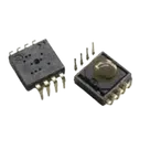
- Package: 8-pin staggered DIP
- Datasheet includes “Figure 3: Recommended PCB Mechanical Cutouts and Spacing” required for proper lens and optical path alignment (dimensions shown graphically in the PDF; numeric values are not tabulated in the version accessed)
- Lens/clip system referenced (e.g., ADNS‑5110‑001 lens, ADNS‑5200 clip)
- Cross-check: symbol and footprint vs datasheet Schematic symbol checks
- Pin count: 8 — matches datasheet.
- Pin names and numbers: Matches exactly (1:MISO, 2:LED, 3:MOTION, 4:NCS, 5:SCLK, 6:GND, 7:VDD, 8:MOSI).
- Pin electrical types: All current terminals are “Unspecified.” Based on the datasheet:
- Signal directionality and logic levels:
- Outputs (MISO, MOTION) have VOH = VDD−0.7 V and VOL = 0.7 V at ±1 mA. Ensure the host logic thresholds are compatible at your chosen VDD.
- Present footprint: df3f2e1e-4727-4f32-990a-225f579bf849.defaultFootprint is a through-hole, 8-pad staggered DIP pattern. This is consistent with the datasheet’s “8‑pin DIP” package.
- Pad mapping: The package asset defines pads 1–8; ensure symbol pin-to-pad mapping follows the datasheet numbering (Pin 1 indicator is present in silk/arc near the top; verify board orientation so Pin 1= MISO).
- Mechanical cutouts/alignment: The datasheet provides a “Recommended PCB Mechanical Cutouts and Spacing” figure required for the optical path and lens/clip seating. The current footprint definition does not include any board cutouts/slots/alignment holes on Edge.Cuts or mechanical layers.
- Action needed: Add the recommended optical aperture and mechanical keep-outs/cutouts per the datasheet figure for the selected lens/clip (e.g., ADNS‑5110‑001 + ADNS‑5200).
- Numerical mechanical dimensions: The accessed PDF shows figures but does not tabulate key values (e.g., pin pitch, body outline, hole locations) in text tables. Before committing to manufacturing, verify pin pitch, row spacing, and hole sizes against a full mechanical drawing from the manufacturer or the lens reference design to confirm pad drills (currently 0.8 mm) and spacing.
- The project’s symbol/footprint align broadly with an 8‑pin DIP ADNS‑3050. The main manufacturing risk is omission of the required PCB optical cutouts and lens alignment geometry. Without them, the sensor will not track correctly.
- Update the symbol pin electrical types as listed.
- Add notes/properties referencing the key electrical limits.
- Create or import a footprint variant that includes the recommended mechanical cutouts aligned to the lens/clip you plan to use.
To get started, talk to Flux or create a New Document.


Welcome 👋
Flux accelerates your PCB design with AI.
Create your account to start using this component and bring your ideas to life.
