Part Data Review and Validation
2:04
I reviewed the part project for TE Connectivity 7-534206-5 and the datasheet URL was already present, so no property update was needed.
Part project summary
| Field | Result |
|---|---|
| MPN | 7-534206-5 |
| Manufacturer | TE Connectivity |
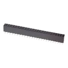
| Project description | 50 MODII VRT DR CE 100/115 |
| Product description | PCB Mount Receptacle, Vertical, Board-to-Board, 50 Position, 2.54 mm centerline, Gold, Through Hole - Solder |
| Series | AMPMODU / Modu Connector System |
| Type | Vertical PCB mount receptacle, socket contacts |
| Positions / rows | 50 positions / 2 rows |
| Pitch | 2.54 mm |
| Row spacing | 2.54 mm |
| Orientation | Vertical |
| Termination | Through Hole - Solder |
| Board retention | Without |
| Board standoff | Yes |
| Contact plating | Gold mating area, Tin termination area |
| Housing / contact features | Closed entry housing, phosphor bronze contacts, top entry |
Symbol / footprint structure found in the project
| Item | Result |
|---|---|
| Symbol pin count | 50 symbol terminals present |
| Footprint pad count | 50 pads present |
| Footprint asset | RHDR50W76P254_2X25_6350X503X813P.kicad_mod |
| 3D model | Present: 7-534206-5.stp |
| Footprint pattern encoded by asset name | 2 x 25, 63.50 x 5.03 x 8.13 mm class |
| Pad numbering | Pads 1...50 exist and map to symbol terminal IDs |
Electrical characteristics
| Parameter | Value |
|---|---|
| Current rating | 3 A max single contact, 2 A per contact fully energized connector |
| Voltage rating | 333 VAC |
| Low level contact resistance | 12 mΩ max |
| Insulation resistance | 5000 MΩ min initial |
| Withstanding voltage | 750 V rms at sea level for .100 CL system |
| Operating temperature | Product page: -65 to 105 °C |
| Temperature rise vs current | 30 °C max at specified current |
| Durability | 200 cycles for 30 µin gold, 100 cycles for 15 µin gold, 25 cycles for 10 µin gold, 75 cycles for 100 µin tin |
Absolute maximum / ratings
| Parameter | Value |
|---|---|
| Current | 3 A max single contact |
| Fully energized current | 2 A per contact max |
| Temperature | Spec page states -65 to 125 °C |
| Withstanding voltage | 750 V rms at sea level for .100 CL |
Recommended operating / application conditions
| Parameter | Value |
|---|---|
| PCB thickness | 1.40 mm to 2.40 mm in application spec |
| Product page operating temp | -65 to 105 °C |
| Placement accuracy for automation | 0.25 mm |
| Max PCB bow | 0.03 mm over connector length |
| Wave solder concerns | Prevent bridging, prevent wicking into receptacles, remove flux after soldering |
| Solderability | 95% minimum solder coverage |
Mechanical / package data
| Parameter | Value |
|---|---|
| Positions / rows | 50 / 2 |
| Pitch | 2.54 mm |
| Row spacing | 2.54 mm from official product page |
| Connector height | 5.03 mm [.198 in] from official product page |
| Termination post length | 2.92 mm [.115 in] |
| Footprint naming dimensions | 63.50 x 5.03 x 8.13 mm encoded in footprint filename |
Pin descriptions
| Item | Result |
|---|---|
| Pin names | Numeric only: 1...50 |
| Pin functional descriptions | No per-pin unique electrical functions found, which is expected for this connector family |
| Numbering note | Customer drawing notes contact numbering is for reference |
Manufacturing / assembly notes
| Topic | Result |
|---|---|
| Solder mask | Recommended between all lands |
| Trace between adjacent lands | Must be solder-mask covered |
| Storage caution | Avoid chemicals that can cause stress corrosion / cracking |
| UV caution | Prolonged UV exposure may degrade housing material |
| Reflow / process | Trial runs recommended under actual manufacturing conditions |
| Through-hole process | Hold-down recommended until soldering completes |
Good matches
| Check | Result |
|---|---|
| Total pin count | Match: symbol 50, footprint 50, product page 50 |
| Row count | Match: footprint asset is 2 x 25, datasheet says 2 rows |
| Pitch family | Match: 2.54 mm |
| Orientation / termination | Match: vertical, through-hole receptacle |
| Overall footprint width class | Match with product page height/width class around 5.03 mm |
Issues flagged
| Severity | Finding | Why it matters |
|---|---|---|
| High | Symbol pins are reported as undefined with Pin Type: Unspecified for all 50 terminals | This can degrade ERC quality and increase risk of incorrect symbol behavior in downstream designs |
| Medium | Project-level designator prefix is J, but symbol terminal properties show Designator Prefix: P | Not a manufacturing failure by itself, but can cause library inconsistency and confusion when instantiating the part |
| High, needs manual confirmation | Footprint file uses 0.95 mm drill and 1.425 mm pad size, while the extracted customer drawing data reported 1.02 mm ± 0.05 mm hole and 1.55 mm min pad diameter | If the drawing extraction is correct, the current footprint may be undersized, creating assembly risk, poor annular ring, or insertion problems |
| Medium | Datasheet sources are internally inconsistent on max operating temperature: product page 105 °C vs spec 125 °C | This is a part-documentation discrepancy that should be resolved before using the part at elevated temperature limits |
- The symbol-to-footprint pin count and numbering coverage look structurally correct.
- The largest possible manufacturing risk is the plated through-hole geometry: current footprint uses 0.95 mm drill / 1.425 mm pad, which may be too small if the official drawing requirement is really 1.02 mm hole / 1.55 mm pad min.
- The symbol metadata quality needs cleanup because all terminals are effectively untyped/undefined.
- I do not see evidence of a catastrophic pin-count mismatch, wrong row count, or wrong connector family.
If you want, I can next produce a concise fix list for this part project.
Create fix checklist
Verify footprint dimensions
Review part issues
58 days


Welcome 👋
Flux accelerates your PCB design with AI.
Create your account to start using this component and bring your ideas to life.