Part Project Metadata Review
1:15
Considering project details.
Analyzing the schematic.
Reviewing the bill of materials.
Analyzing the PCB layout.
Looking for "part description and product overview" in 5051106491_sd.pdf
Looking for "circuits count and contact count" in 5051106491_sd.pdf
Looking for "pitch, height, orientation, contact style, plating, series, product family" in 5051106491_sd.pdf
Looking for "electrical characteristics including voltage rating current rating contact resistance insulation resistance dielectric withstanding voltage operating temperature" in 5051106491_sd.pdf
Looking for "absolute maximum ratings or maximum voltage current temperature mechanical limits" in 5051106491_sd.pdf
Looking for "recommended operating conditions or normal use conditions" in 5051106491_sd.pdf
Looking for "pin numbering and contact arrangement" in 5051106491_sd.pdf
Looking for "mounting pad layout recommended pcb pattern dimensions" in 5051106491_sd.pdf
Looking for "mechanical dimensions overall length width height and package dimensions" in 5051106491_sd.pdf
Looking for "special features locking actuator easy on fd19 bottom contact right angle gold over nickel" in 5051106491_sd.pdf
Checking symbol and footprint alignment.
Project metadata summary
| Field | Result |
|---|---|
| MPN | 505110-6491 |
| Manufacturer | Molex |
| Part type | Connector |
| Series | 505110 |
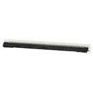
| Description | Easy-On FFC/FPC Connector, 0.50 mm pitch, right-angle, bottom contact |
| Stated height in project | 1.90 mm |
| Circuits / contacts | 64 |
| Datasheet URL present | Yes |
| Datasheet URL | https://www.molex.com/pdm_docs/sd/5051106491_sd.pdf |
| Schematic terminals present | 66 total = signal pads 1 through 64, plus mounting pads MP1 and MP2 |
| Footprint asset | 5051106491.kicad_mod |
| 3D model asset | 505110-6491.stp |
Core part metadata
| Parameter | Datasheet result |
|---|---|
| Product family | FFC/FPC connector |
| Series | 505110 |
| Orientation | Right-angle |
| Contact style | Bottom contact, ZIF |
| Pitch | 0.5 mm |
| Circuit count | 64 |
| Packaging | Embossed tape on reel |
| Contact plating | Gold over nickel |
| Fitting nail plating | Tin over nickel |
Electrical characteristics
| Parameter | Datasheet result |
|---|---|
| Voltage rating | 50 V AC (RMS) / DC |
| Current rating | 0.5 A |
| Contact resistance | 40 mΩ max |
| Insulation resistance | 100 MΩ min |
| Dielectric withstanding voltage | 250 V AC for 1 minute |
| Operating temperature | -40 to +105 °C |
Absolute maximum ratings / limits
| Item | Datasheet result |
|---|---|
| Explicit absolute max table | Not found in the PDF extraction |
| Extracted mechanical limit | Tails and nails coplanarity: 0.1 mm max |
Recommended operating conditions
| Item | Result |
|---|---|
| Explicit recommended operating conditions table | Not clearly present in the extracted PDF text |
| Usable operating range found | -40 to +105 °C |
Pin descriptions
Package / recommended PCB dimensions extracted
| Item | Datasheet result |
|---|---|
| Signal pad pitch | 0.5 ± 0.05 mm |
| Signal pad width | 0.3 ± 0.05 mm |
| Signal pad length | 1.0 ± 0.05 mm |
| Mounting pad width | 1.3 ± 0.05 mm |
| Mounting pad length | 2.0 mm class dimension appears in the recommended layout extraction |
| Row span formula | 0.5 (N-1) ± 0.05 mm |
| Other extracted recommended pattern dims | 1.55 ± 0.05 mm, 3.3 ± 0.05 mm, 2.6, 2.0 |
Special features
| Feature | Result |
|---|---|
| Connector type | Easy-On FFC/FPC |
| Insertion style | ZIF |
| Contact orientation | Bottom contact |
| Mounting style | Right-angle SMT |
| Retention | Mechanical fitting nails / hold-down pads |
| Plating | Gold over nickel on contacts |
What matches
| Check | Result | Notes |
|---|---|---|
| Signal pin count | Pass | Schematic has 1-64 |
| Mechanical pad count | Pass | Schematic includes MP1 and MP2 |
| Total terminal count | Pass | 66 total pads represented |
| Footprint signal pad pitch | Pass | Footprint pads are on 0.5 mm pitch |
| Footprint signal pad size | Pass | Footprint uses 0.30 mm x 1.00 mm |
| Footprint contact span | Pass | Pad 1 to 64 span is 31.5 mm, matching 0.5 x (64-1) |
| Footprint mounting pad size | Likely pass | Footprint uses 1.3 mm x 2.0 mm for MP1 and MP2 |
| Mechanical pads included | Pass | Good for manufacturability and retention |
| 3D model present | Pass | Helpful for enclosure/mechanical validation |
Issues / risks found
| Issue | Severity | Why it matters |
|---|---|---|
| Project description says 1.90 mm height, but extracted PDF text returned 2.0 mm height | Medium | Could cause enclosure or mating-height mistakes and wrong part ordering if the description is used as the source of truth |
| All schematic terminals are typed Unspecified | Low to Medium | Not a fab blocker, but poor metadata quality for a reusable part |
| Schematic terminals use prefix P internally while project designator prefix is J | Low | Usually harmless in a part project, but inconsistent metadata |
| No explicit pin role metadata for mounting pads MP1 and MP2 | Medium | Could confuse downstream users; these should clearly be mechanical shield / hold-down style terminals, not generic signal pins |
| No explicit footprint-side / orientation note surfaced in the symbol metadata | Medium | Bottom-contact FFC connectors are easy to place backward in end-use designs if the symbol/documentation is not very explicit |
Overall assessment
| Area | Verdict |
|---|---|
| Pin count and pad count | Good |
| Footprint geometry vs extracted recommended layout | Looks correct |
| Manufacturing risk from footprint | Low |
| Risk of ordering / mechanical misunderstanding | Moderate |
| Most important cleanup item | Resolve the 1.90 mm vs 2.0 mm height discrepancy and make bottom-contact orientation more explicit |
- The footprint itself looks consistent with a 64-pin, 0.5 mm pitch Molex connector and includes both mounting pads MP1 and MP2.
- The biggest concern is metadata accuracy, not pad geometry:
- Height mismatch in project description vs extracted datasheet text
- Unspecified pin types
- Mounting pads not clearly labeled as mechanical
- Bottom-contact behavior not strongly encoded in part metadata
Ready.
Reviews

- Wirelessly connects nets on schematic. Used to organize schematics and separate functional blocks. To wirelessly connect net portals, give them same designator. #portaljharwinbarrozo43.0M
- Wirelessly connects power nets on schematic. Identical to the net portal, but with a power symbol. Used to organize schematics and separate functional blocks. To wirelessly connect power net portals, give them the same designator. #portal #powerjharwinbarrozo11.4M
- A generic fixed resistor ideal for rapid circuit topology development. Its footprint automatically adapts based on the selected package case code—supporting 0402, 0603, 0805, 1203, and many other standard SMD packages, as well as axial horizontal and vertical configurations. Save precious design time by seamlessly add more information to this part (value, footprint, etc.) as it becomes available. Standard resistor values: 1.0 ohm, 10 ohm, 100 ohm, 1.0k ohm, 10k ohm, 100k ohm, 1.0M ohm 1.1 ohm, 11 ohm, 110 ohm, 1.1k ohm, 11k ohm, 110k ohm, 1.1M ohm 1.2 ohm, 12 ohm, 120 ohm, 1.2k ohm, 12k ohm, 120k ohm, 1.2M ohm 1.3 ohm, 13 ohm, 130 ohm, 1.3k ohm, 13k ohm, 130k ohm, 1.3M ohm 1.5 ohm, 15 ohm, 150 ohm, 1.5k ohm, 15k ohm, 150k ohm, 1.5M ohm 1.6 ohm, 16 ohm, 160 ohm, 1.6k ohm, 16k ohm, 160k ohm, 1.6M ohm 1.8 ohm, 18 ohm, 180 ohm, 1.8K ohm, 18k ohm, 180k ohm, 1.8M ohm 2.0 ohm, 20 ohm, 200 ohm, 2.0k ohm, 20k ohm, 200k ohm, 2.0M ohm 2.2 ohm, 22 ohm, 220 ohm, 2.2k ohm, 22k ohm, 220k ohm, 2.2M ohm 2.4 ohm, 24 ohm, 240 ohm, 2.4k ohm, 24k ohm, 240k ohm, 2.4M ohm 2.7 ohm, 27 ohm, 270 ohm, 2.7k ohm, 27k ohm, 270k ohm, 2.7M ohm 3.0 ohm, 30 ohm, 300 ohm, 3.0K ohm, 30K ohm, 300K ohm, 3.0M ohm 3.3 ohm, 33 ohm, 330 ohm, 3.3k ohm, 33k ohm, 330k ohm, 3.3M ohm 3.6 ohm, 36 ohm, 360 ohm, 3.6k ohm, 36k ohm, 360k ohm, 3.6M ohm 3.9 ohm, 39 ohm, 390 ohm, 3.9k ohm, 39k ohm, 390k ohm, 3.9M ohm 4.3 ohm, 43 ohm, 430 ohm, 4.3k ohm, 43K ohm, 430K ohm, 4.3M ohm 4.7 ohm, 47 ohm, 470 ohm, 4.7k ohm, 47k ohm, 470k ohm, 4.7M ohm 5.1 ohm, 51 ohm, 510 ohm, 5.1k ohm, 51k ohm, 510k ohm, 5.1M ohm 5.6 ohm, 56 ohm, 560 ohm, 5.6k ohm, 56k ohm, 560k ohm, 5.6M ohm 6.2 ohm, 62 ohm, 620 ohm, 6.2k ohm, 62K ohm, 620K ohm, 6.2M ohm 6.8 ohm, 68 ohm, 680 ohm, 6.8k ohm, 68k ohm, 680k ohm, 6.8M ohm 7.5 ohm, 75 ohm, 750 ohm, 7.5k ohm, 75k ohm, 750k ohm, 7.5M ohm 8.2 ohm, 82 ohm, 820 ohm, 8.2k ohm, 82k ohm, 820k ohm, 8.2M ohm 9.1 ohm, 91 ohm, 910 ohm, 9.1k ohm, 91k ohm, 910k ohm, 9.1M ohm #generics #CommonPartsLibraryjharwinbarrozo1.5M
- A generic fixed capacitor ideal for rapid circuit topology development. You can choose between polarized and non-polarized types, its symbol and the footprint will automatically adapt based on your selection. Supported options include standard SMD sizes for ceramic capacitors (e.g., 0402, 0603, 0805), SMD sizes for aluminum electrolytic capacitors, and through-hole footprints for polarized capacitors. Save precious design time by seamlessly add more information to this part (value, footprint, etc.) as it becomes available. Standard capacitor values: 1.0pF, 10pF, 100pF, 1000pF, 0.01uF, 0.1uF, 1.0uF, 10uF, 100uF, 1000uF, 10000uF 1.1pF, 11pF, 110pF, 1100pF 1.2pF, 12pF, 120pF, 1200pF 1.3pF, 13pF, 130pF, 1300pF 1.5pF, 15pF, 150pF, 1500pF, 0.015uF, 0.15uF, 1.5uF, 15uF, 150uF, 1500uF 1.6pF, 16pF, 160pF, 1600pF 1.8pF, 18pF, 180pF, 1800pF 2.0pF, 20pF, 200pF, 2000pF 2.2pF, 22pF, 220pF, 2200pF, 0.022uF, 0.22uF, 2.2uF, 22uF, 220uF, 2200uF 2.4pF, 24pF, 240pF, 2400pF 2.7pF, 27pF, 270pF, 2700pF 3.0pF, 30pF, 300pF, 3000pF 3.3pF, 33pF, 330pF, 3300pF, 0.033uF, 0.33uF, 3.3uF, 33uF, 330uF, 3300uF 3.6pF, 36pF, 360pF, 3600pF 3.9pF, 39pF, 390pF, 3900pF 4.3pF, 43pF, 430pF, 4300pF 4.7pF, 47pF, 470pF, 4700pF, 0.047uF, 0.47uF, 4.7uF, 47uF, 470uF, 4700uF 5.1pF, 51pF, 510pF, 5100pF 5.6pF, 56pF, 560pF, 5600pF 6.2pF, 62pF, 620pF, 6200pF 6.8pF, 68pF, 680pF, 6800pF, 0.068uF, 0.68uF, 6.8uF, 68uF, 680uF, 6800uF 7.5pF, 75pF, 750pF, 7500pF 8.2pF, 82pF, 820pF, 8200pF 9.1pF, 91pF, 910pF, 9100pF #generics #CommonPartsLibraryjharwinbarrozo1.5M
- A generic fixed inductor suitable for rapid circuit topology development. The footprint automatically adapts based on the selected package, supporting standard SMD sizes (e.g., 0402, 0603, 0805) as well as well-known inductor packages such as SDR1806, PA4320, SRN6028, and SRR1260. Standard inductor values: 1.0 nH, 10 nH, 100 nH, 1.0 µH, 10 µH, 100 µH, 1.0 mH 1.2 nH, 12 nH, 120 nH, 1.2 µH, 12 µH, 120 µH, 1.2 mH 1.5 nH, 15 nH, 150 nH, 1.5 µH, 15 µH, 150 µH, 1.5 mH 1.8 nH, 18 nH, 180 nH, 1.8 µH, 18 µH, 180 µH, 1.8 mH 2.2 nH, 22 nH, 220 nH, 2.2 µH, 22 µH, 220 µH, 2.2 mH 2.7 nH, 27 nH, 270 nH, 2.7 µH, 27 µH, 270 µH, 2.7 mH 3.3 nH, 33 nH, 330 nH, 3.3 µH, 33 µH, 330 µH, 3.3 mH 3.9 nH, 39 nH, 390 nH, 3.9 µH, 39 µH, 390 µH, 3.9 mH 4.7 nH, 47 nH, 470 nH, 4.7 µH, 47 µH, 470 µH, 4.7 mH 5.6 nH, 56 nH, 560 nH, 5.6 µH, 56 µH, 560 µH, 5.6 mH 6.8 nH, 68 nH, 680 nH, 6.8 µH, 68 µH, 680 µH, 6.8 mH 8.2 nH, 82 nH, 820 nH, 8.2 µH, 82 µH, 820 µH, 8.2 mH #generics #CommonPartsLibraryjharwinbarrozo15.6k
- An electrical connector acting as reusable interface to a conductor and creating a point where external circuits can be connected.Terminal
- 47 kOhms ±5% 0.125W, 1/8W Chip Resistor 0805 (2012 Metric) Automotive AEC-Q200 Thick Film #forLedBlinkjharwinbarrozo1.2M
- 10uF Capacitor Aluminum Polymer 20% 16V SMD 5x5.3mm #forLedBlink #commonpartslibrary #capacitor #aluminumpolymer #radialcanjharwinbarrozo1.2M
- Yellow 595nm LED Indication - Discrete 1.7V 1206 (3216 Metric) #forLedBlinkjharwinbarrozo1.1M


5051106491
Properties
5051106491
Molex
Connectors
J
Pricing & Availability
See prices from popular manufacturers for your project.
Assets

505110-6491
505110-6491 Symbol.svgDefault505110-6491
5051106491.kicad_modFootprint505110-6491
505110-6491.stp3D Model
5051106491-thumb.png
5051106491-thumbThumbnailControls
Welcome 👋
Flux accelerates your PCB design with AI.
Create your account to start using this component and bring your ideas to life.