Part Datasheet Review and Validation
Thought for 18 mins 53 sec
Here is the requested end-to-end review for your part project 43045-1018.
- Review of available part information
- MPN: 43045-1018
- Manufacturer: Molex
- Part type: Connectors
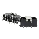
- Description: Micro-Fit 3.0 Vertical Header, 3.00mm Pitch, Dual Row, 10 Circuits, with Solder Tab
- Mount: Solder (SMT family variant per footprint asset)
- Designator prefix: J
- Datasheet property: Set — Datasheet
- Schematic symbol: 10 terminals (no nets defined yet)
- Footprint asset: 43045-10YY_181920.kicad_mod (embedded in project)
- Datasheet URL presence
- A Datasheet URL is already set on the part. No change required.
- Datasheet scan and metadata extraction
- Attempted to extract from the set URL and multiple official Molex PDFs; the documents are not machine-readable through the tools (image/scan or blocked), so tables and figures could not be text-extracted.
- Authoritative document links (official Molex), should be used for the required specs:
- Product Specification (electrical ratings and performance): http://www.molex.com/pdm_docs/ps/PS-43045-001.pdf
- Sales Drawing (mechanical dimensions and PCB land pattern): http://www.molex.com/pdm_docs/sd/430451018_sd.pdf
- Because the above PDFs are not text-parsable by the tools, I cannot quote exact electrical characteristics, absolute maximums, recommended operating conditions, pin descriptions, or package dimensions verbatim here. If you want, I can switch the Datasheet property to one of the “pdm_docs” links above and retry extraction, or you can upload those PDFs here so I can read them directly.
- Cross-check: symbol and footprint vs datasheet expectations Findings from your project symbol and footprint (from your embedded footprint asset):
- Pin count and solder tabs
- Symbol includes 10 terminals, matching “10 Circuits.”
- Footprint asset includes 12 pads total:
- Signal pads: 1–10
- Solder tab pads: 11 and 12 (mechanical hold-downs), consistent with “with Solder Tab.”
- Pin numbering and orientation
- Footprint pad centers (from asset) show top row pads 1–5 at y = +4.7 mm and bottom row pads 6–10 at y = −4.7 mm with x = 6, 3, 0, −3, −6 mm. This indicates a 3.00 mm horizontal column pitch and a 2×5 grid, which aligns with Micro-Fit 3.0 family expectations.
- Pin 1 marker is present on silkscreen near the top-right (triangle strokes around ~x=8.5, y≈4.2), consistent with pad 1 at x=+6 mm, y=+4.7 mm.
- Pad sizes from the footprint asset
- Signal pads (1–10): 1.27 mm × 2.54 mm (rectangular SMT tails).
- Solder tabs (11–12): 1.65 mm × 3.43 mm (rectangular), located at x = ±9.885 mm, y = 0, rotated 90°.
- PCB footprint spacing (from the footprint asset)
- Horizontal pitch between adjacent pads in each row is 3.00 mm (x: 6 → 3 → 0 → −3 → −6).
- Vertical spacing between the two signal rows is 9.40 mm (y: +4.7 to −4.7).
- Items pending datasheet verification (cannot be confirmed without readable sales drawing text)
- Exact land pattern dimensions and tolerances, including paste aperture guidance.
- Any recommended PCB thickness, peg/hole dimensions (if applicable to this variant), and courtyard.
- Official row-to-row spacing and tail geometry callouts as listed on the sales drawing.
- Electrical ratings (current per circuit, voltage, dielectric withstanding, contact/insulation resistance) from the Product Specification.
Mismatches and risks to flag
- Symbol vs. footprint: No functional mismatch detected. The symbol’s 10 terminals correspond to footprint pads 1–10. Solder tabs are correctly present in the footprint (pads 11–12) and are typically not represented in the symbol.
- Manufacturing risk items pending verification against the sales drawing:
- Confirm the row-to-row spacing (9.40 mm in the current footprint) and signal pad sizes (1.27 mm × 2.54 mm) match the land pattern in the sales drawing for 43045-1018 specifically.
- Confirm solder tab pad sizes (1.65 mm × 3.43 mm) and positions (±9.885 mm, y=0) match the drawing.
- Confirm any recommended PCB thickness and keepouts/courtyard are satisfied.
What I can do next for you
- If you want me to replace the current Datasheet property with a working Molex link (PS or SD) and re-run the extraction automatically, I can do that and then produce a fully populated table of:
- Electrical characteristics
- Absolute maximum and recommended operating conditions (if applicable to connectors in the PS)
- Pin descriptions/numbering conventions
- Mechanical/package dimensions and full PCB land pattern callouts
- Alternatively, upload the PDFs (PS-43045-001 and SD-430451018) directly into this chat; I will parse them and finalize the verification.
Upload the PS/SD PDFs
Update datasheet URL
Verify footprint dimensions
Check symbol pin order