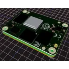
Diseño de PCB para Raspberry Pi CM4
0:00
Work completed
- Project description updated to detail PCIe cellular slot integration
- System architecture property set with CM4, PCIe slot, power, USB, SIM, and antenna subsystems
- J3 placed with mounting holes and keep-out zone
- Ground portal symbol added
- U1 ESD array added for SIM/UIM
- U2 switched 3.3 V rail controller with enable/reset
- C1 and C2 decoupling capacitors placed
- D1 and D2 TVS diodes added at regulator output and connector power pins
Tasks remaining
- Select and place AC-coupling Capacitor and Common-mode Choke for PCIe/USB lanes
- Select and add Nano-SIM Holder and u.FL Connector
- Connect all nets:
- PCIe differential pairs, REFCLK, PERST# via AC-coupling & chokes
- USB2.0 D+/D– from hub to socket
- SIM/UIM through ESD array to nano-SIM holder
- 3.3 V rail and enable/reset to socket and regulator
- Review schematic for completeness and electrical requirements
- Verify passive/active ratings and footprints
- Configure PCB stackup, copper layers, and ground fill
- Define mechanical mounting holes and clearance
- Perform DRC and length-match checks
Success criteria
- The PCIe slot socket is placed but nets aren’t yet routed; supporting I/O, power, SIM, and antenna connectors are pending. Signal-integrity, EMI/ESD compliance, and board-size fit remain to be validated.
Next step
Pick and add the AC-coupling capacitors and common-mode chokes for the PCIe and USB lanes.
148 days
Ready.
J2
J1
Reviews

- Wirelessly connects nets on schematic. Used to organize schematics and separate functional blocks. To wirelessly connect net portals, give them same designator. #portaljharwinbarrozo43.0M
- Wirelessly connects power nets on schematic. Identical to the net portal, but with a power symbol. Used to organize schematics and separate functional blocks. To wirelessly connect power net portals, give them the same designator. #portal #powerjharwinbarrozo11.4M
- A generic fixed resistor for rapid developing circuit topology. Save precious design time by seamlessly add more information to this part (value, footprint, etc.) as it becomes available. Standard resistor values: 1.0Ω 10Ω 100Ω 1.0kΩ 10kΩ 100kΩ 1.0MΩ 1.1Ω 11Ω 110Ω 1.1kΩ 11kΩ 110kΩ 1.1MΩ 1.2Ω 12Ω 120Ω 1.2kΩ 12kΩ 120kΩ 1.2MΩ 1.3Ω 13Ω 130Ω 1.3kΩ 13kΩ 130kΩ 1.3MΩ 1.5Ω 15Ω 150Ω 1.5kΩ 15kΩ 150kΩ 1.5MΩ 1.6Ω 16Ω 160Ω 1.6kΩ 16kΩ 160kΩ 1.6MΩ 1.8Ω 18Ω 180Ω 1.8KΩ 18kΩ 180kΩ 1.8MΩ 2.0Ω 20Ω 200Ω 2.0kΩ 20kΩ 200kΩ 2.0MΩ 2.2Ω 22Ω 220Ω 2.2kΩ 22kΩ 220kΩ 2.2MΩ 2.4Ω 24Ω 240Ω 2.4kΩ 24kΩ 240kΩ 2.4MΩ 2.7Ω 27Ω 270Ω 2.7kΩ 27kΩ 270kΩ 2.7MΩ 3.0Ω 30Ω 300Ω 3.0KΩ 30KΩ 300KΩ 3.0MΩ 3.3Ω 33Ω 330Ω 3.3kΩ 33kΩ 330kΩ 3.3MΩ 3.6Ω 36Ω 360Ω 3.6kΩ 36kΩ 360kΩ 3.6MΩ 3.9Ω 39Ω 390Ω 3.9kΩ 39kΩ 390kΩ 3.9MΩ 4.3Ω 43Ω 430Ω 4.3kΩ 43KΩ 430KΩ 4.3MΩ 4.7Ω 47Ω 470Ω 4.7kΩ 47kΩ 470kΩ 4.7MΩ 5.1Ω 51Ω 510Ω 5.1kΩ 51kΩ 510kΩ 5.1MΩ 5.6Ω 56Ω 560Ω 5.6kΩ 56kΩ 560kΩ 5.6MΩ 6.2Ω 62Ω 620Ω 6.2kΩ 62KΩ 620KΩ 6.2MΩ 6.8Ω 68Ω 680Ω 6.8kΩ 68kΩ 680kΩ 6.8MΩ 7.5Ω 75Ω 750Ω 7.5kΩ 75kΩ 750kΩ 7.5MΩ 8.2Ω 82Ω 820Ω 8.2kΩ 82kΩ 820kΩ 8.2MΩ 9.1Ω 91Ω 910Ω 9.1kΩ 91kΩ 910kΩ 9.1MΩ #generics #CommonPartsLibraryjharwinbarrozo1.5M
- A generic fixed capacitor ideal for rapid circuit topology development. You can choose between polarized and non-polarized types, its symbol and the footprint will automatically adapt based on your selection. Supported options include standard SMD sizes for ceramic capacitors (e.g., 0402, 0603, 0805), SMD sizes for aluminum electrolytic capacitors, and through-hole footprints for polarized capacitors. Save precious design time by seamlessly add more information to this part (value, footprint, etc.) as it becomes available. Standard capacitor values: 1.0pF 10pF 100pF 1000pF 0.01uF 0.1uF 1.0uF 10uF 100uF 1000uF 10,000uF 1.1pF 11pF 110pF 1100pF 1.2pF 12pF 120pF 1200pF 1.3pF 13pF 130pF 1300pF 1.5pF 15pF 150pF 1500pF 0.015uF 0.15uF 1.5uF 15uF 150uF 1500uF 1.6pF 16pF 160pF 1600pF 1.8pF 18pF 180pF 1800pF 2.0pF 20pF 200pF 2000pF 2.2pF 22pF 20pF 2200pF 0.022uF 0.22uF 2.2uF 22uF 220uF 2200uF 2.4pF 24pF 240pF 2400pF 2.7pF 27pF 270pF 2700pF 3.0pF 30pF 300pF 3000pF 3.3pF 33pF 330pF 3300pF 0.033uF 0.33uF 3.3uF 33uF 330uF 3300uF 3.6pF 36pF 360pF 3600pF 3.9pF 39pF 390pF 3900pF 4.3pF 43pF 430pF 4300pF 4.7pF 47pF 470pF 4700pF 0.047uF 0.47uF 4.7uF 47uF 470uF 4700uF 5.1pF 51pF 510pF 5100pF 5.6pF 56pF 560pF 5600pF 6.2pF 62pF 620pF 6200pF 6.8pF 68pF 680pF 6800pF 0.068uF 0.68uF 6.8uF 68uF 680uF 6800uF 7.5pF 75pF 750pF 7500pF 8.2pF 82pF 820pF 8200pF 9.1pF 91pF 910pF 9100pF #generics #CommonPartsLibraryjharwinbarrozo1.5M
- A generic fixed inductor for rapid developing circuit topology. *You can now change the footprint and 3D model at the top level anytime you want. This is the power of #genericsjharwinbarrozo15.5k
- An electrical connector acting as reusable interface to a conductor and creating a point where external circuits can be connected.Terminal
- 47 kOhms ±5% 0.125W, 1/8W Chip Resistor 0805 (2012 Metric) Automotive AEC-Q200 Thick Film #forLedBlinkjharwinbarrozo1.2M
- 10uF Capacitor Aluminum Polymer 20% 16V SMD 5x5.3mm #forLedBlink #commonpartslibrary #capacitor #aluminumpolymer #radialcanjharwinbarrozo1.2M
- Yellow 595nm LED Indication - Discrete 1.7V 1206 (3216 Metric) #forLedBlinkjharwinbarrozo1.1M


Welcome 👋
Flux helps you build PCBs faster with an AI teammate!
Create your account to collaborate, stay updated, fork your own version, and get instant answers from our AI agent.