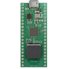
Do a deep dive into this project and come up with...
Thinking for 4 days 15 hrs...
Thought for a moment — Gathering datasheet details
Search "Identify the power architecture of this project. L...".
Running 4 design checks.
Reading BOM for U1, U2, U3 and 10 more.
Reading schematic for U1, U2, U3 and 18 more.
Reading schematic for R1, R2, R3 and 63 more.
Thought for a moment — Identifying major loads on each rail
Search project.
Search project.
Search For DMG1012T, provide Rds(on), continuous drain current, leakage current, and any gate leakage relevant to estimating series power-path current loss.%2C%20continuous%20drain%20current%2C%20leakage%20current%2C%20and%20any%20gate%20leakage%20relevant%20to%20estimating%20series%20power-path%20current%20loss.).
Reading schematic for Power Net Portal.
Thought for a moment — Considering R5/R6 Divider
Search project.
Thought for a moment — Understanding VBUS to VSYS connection
Search project.
Thought for a moment — Investigating power architecture
Search project.
Running code.
Code executed.
Running code.
Code executed.
Prompt: import pandas as pd
rows = [
['Board rail','VBUS','USB connector J3 pin 1','D1->VSYS power path + R11/R12 VBUS sense divider','5 V nominal','0.446 mA divider + downstream VSYS load','0.491 mA divider + all VSYS input demand','R11=5.6k, R12=5.6k; I=V/R','Derived from schematic; board datasheet says VBUS feeds VSYS through D1'],
['Board rail','VSYS','D1 from VBUS or external supply','U2 VIN/VINA, 3V3_EN pull-up, VSYS ADC monitor path','~1.8 V to 5.5 V','Regulator input current + 0 to 0.167 mA monitor overhead','Depends on 3V3 load; divider path 0.183 mA max when Q1 on','R15=20k, R17=10k gated divider; board datasheet range 1.8 to 5.5 V','Direct board-datasheet rail range; total current requires load/efficiency assumption'],
['Board rail','+3V3 main rail','U2 RT6154 buck-boost output','U1 3.3 V domains, U3 flash, CYW43439 input island via FB1, feedback divider, exported 3V3 pin','3.3 V','Design-dependent; dominated by CYW43439 mode and RP2350 activity','~660 mA internal-only conservative stack-up before external 3V3 pin load','U4 Wi-Fi TX 320 mA + U1 VREG_LX max 200 mA + U1 IOVDD max 100 mA + U1 QSPI_IOVDD max 20 mA + U3 active max 20 mA + U2 IQ 0.04 mA + FB divider 0.005 mA','Very conservative non-simultaneous stack-up; board datasheet recommends external 3V3 load under 300 mA'],
['Local rail','+1V1','U1 internal SMPS/LDO via L1','RP2350 DVDD core domain','1.1 V nominal','Not directly specified as a whole-chip typical','200 mA max','RP2350 VREG_LX max current 200 mA','Direct datasheet limit; not actual operating current'],
['Local rail','ADC_AVDD','+3V3 through R2','RP2350 ADC analog supply','3.3 V nominal','Not explicitly given on ADC_AVDD pin; ADC block baseline 0.14 mA noted','Not separately specified','R2=1 ohm feed; datasheet notes ADC block baseline current 0.14 mA and ADC performance degrades below 2.97 V','Partial datasheet coverage only'],
['Local rail','VREG_AVDD','+3V3 through R5','RP2350 internal regulator analog supply','3.3 V nominal','Not separately specified','Bounded indirectly by 1V1 rail max 200 mA output','R5=33 ohm feed to VREG_AVDD','No explicit VREG_AVDD pin current found'],
['Local rail','QSPI_IOVDD','+3V3 main rail','RP2350 QSPI I/O bank','1.8 V to 3.3 V allowed; schematic uses 3.3 V','Mode-dependent','20 mA max source current / 20 mA max sink current','RP2350 QSPI_IOVDD absolute current limits','Direct datasheet pin-domain limit'],
['Local rail','IOVDD aggregate','+3V3 main rail','RP2350 GPIO banks','1.8 V to 3.3 V allowed; schematic uses 3.3 V','Mode-dependent','100 mA total source current / 100 mA total sink current','RP2350 total IOVDD/IOVSS current limits','Direct datasheet GPIO-domain limit'],
['Local rail','USB_OTP_VDD','+3V3 main rail','RP2350 USB PHY + OTP domain','3.3 V nominal','Must always be powered; no separate rail current given','USBCTRL block baseline 1.25 mA noted','RP2350 datasheet USBCTRL baseline current','Block current, not a dedicated pin current'],
['Local rail','W25Q32 VCC','+3V3 main rail','U3 QSPI flash','2.7 V to 3.6 V','6 to 11 mA active read typ depending on clock; 0.01 mA standby typ; 0.0001 mA deep power-down typ','20 mA active read max; 15 mA program/erase max; 0.06 mA standby max','Winbond datasheet ICC values','Direct datasheet values'],
['Local rail','VDDBAT / CYW43439 input island','+3V3 through FB1','U4 VBAT and VDDIO input pins and internal PMU','3.3 V used in schematic','Sleep ~0.006 mA to RX ~37 to 43 mA to BT active ~11.8 to 29.1 mA','Wi-Fi TX 320 mA at 19.5 dBm','CYW43439 VBAT current table; FB1 isolates island','Direct datasheet current table'],
['Internal U4 rail','VOUT_3P3','CYW43439 internal LDO3P3','WLRF_PA_VDD through R23 plus local decoupling','3.3 V','200 mA average path rating; PA rail 75 mA average','450 to 800 mA peak on LDO3P3; PA branch 92 mA peak','CYW43439 power topology figures','Topology-figure values, not all conditions simultaneously'],
['Internal U4 rail','VOUT_LNLDO / core island','CYW43439 internal LNLDO','VDDC rails, WLRF_VDD_1P35 path via L4','1.2 V output, 1.35 V intermediate domain shown','100 mA nominal LNLDO rating','150 mA max; downstream VCO LDO up to 200 mA max noted','CYW43439 topology values','Topology figure; exact net split across VOUT_CORE/VOUT_LN needs schematic interpretation'],
['Internal U4 rail','VOUT_CLDO / 1.2 V island','CYW43439 CLLDO via FB2','BT_VCO_VDD, FM_RF_VDD, BT_IF_VDD, BTFM_PLL_VDD; XTAL 1.2 V via FB2 branch','1.3 V / 1.2 V / 0.95 V selectable (AVS)','80 mA average','200 mA peak','CYW43439 CLDO ratings','Direct topology figure values'],
['Internal U4 rail','WLRF_XTAL_VDD1P2','Internal LP LDO1 via FB2 branch','WLRF crystal supply','1.2 V','Not separately given','5 mA rated','CYW43439 LP LDO1 rating','Direct topology figure value'],
['Feedback / divider','U2 FB divider','+3V3 to FB to GND via R24/R25','RT6154 output feedback network','3.3 V -> 0.5 V FB','5.0 uA','5.0 uA nominally; leakage adds ±1 uA worst-case uncertainty','R24=560k, R25=100k, VFB=0.5 V','Resistor current derived from schematic; FB leakage ±1 uA max from datasheet'],
['Feedback / control','U2 EN pull-up','VSYS through R8','RT6154 enable bias','VSYS','~0 A when left high; only pin leakage','Pin leakage negligible; if externally forced low, about 55 uA through 100k at 5.5 V','R8=100k, EN high by default','No explicit EN input current found; estimate from resistor only'],
['Feedback / control','U2 PS/SYNC control','GPIO via R9? direct net control','Mode / sync control','Logic level','0.1 uA typ','1 uA max','RT6154 PS/SYNC pin current spec','Direct datasheet value'],
['Feedback / control','U2 PGOOD output','Open-drain output','Status only; currently floating in schematic review','Logic/open drain','0.01 uA leakage typ','0.1 uA leakage max','RT6154 PGOOD leakage spec','Direct datasheet value; ERC flags PGOOD floating'],
['Sense divider','VBUS monitor divider','VBUS through R11/R12','U4 GPIO_2 VBUS detect','5 V nominal','0.446 mA','0.491 mA at 5.5 V','R11=5.6k, R12=5.6k','Pure schematic-derived current'],
['Sense divider','VSYS monitor divider','VSYS through R15/Q1/R17','U1 ADC3 battery monitor path','VSYS / 3 at ADC when Q1 on','0.167 mA at 5.0 V when enabled','0.183 mA at 5.5 V when enabled; ~0 when Q1 off except leakage','R15=20k, R17=10k, Q1 gates divider','Derived from schematic and board-datasheet function note'],
['Signal load','LED branch (GPIO-powered)','RP2350 GPIO through R18 to LED1 to GND','Status LED, not a dedicated power net load','3.3 V logic high assumed','~7.0 mA upper-bound ignoring LED Vf','Lower in reality after LED forward drop; exact depends on LED Vf','3.3 V / 470 ohm = 7.0 mA ideal upper bound','Schematic-derived; LED Vf missing']
]
cols=['Section','Rail/Section','Source','Consumers / section','Voltage','Typ current','Worst-case current','Basis','Datasheet / source flag']
df=pd.DataFrame(rows, columns=cols)
print(df.to_csv(index=False))
Result: Section,Rail/Section,Source,Consumers / section,Voltage,Typ current,Worst-case current,Basis,Datasheet / source flag
Board rail,VBUS,USB connector J3 pin 1,D1->VSYS power path + R11/R12 VBUS sense divider,5 V nominal,0.446 mA divider + downstream VSYS load,0.491 mA divider + all VSYS input demand,"R11=5.6k, R12=5.6k; I=V/R",Derived from schematic; board datasheet says VBUS feeds VSYS through D1
Board rail,VSYS,D1 from VBUS or external supply,"U2 VIN/VINA, 3V3_EN pull-up, VSYS ADC monitor path",~1.8 V to 5.5 V,Regulator input current + 0 to 0.167 mA monitor overhead,Depends on 3V3 load; divider path 0.183 mA max when Q1 on,"R15=20k, R17=10k gated divider; board datasheet range 1.8 to 5.5 V",Direct board-datasheet rail range; total current requires load/efficiency assumption
Board rail,+3V3 main rail,U2 RT6154 buck-boost output,"U1 3.3 V domains, U3 flash, CYW43439 input island via FB1, feedback divider, exported 3V3 pin",3.3 V,Design-dependent; dominated by CYW43439 mode and RP2350 activity,~660 mA internal-only conservative stack-up before external 3V3 pin load,U4 Wi-Fi TX 320 mA + U1 VREG_LX max 200 mA + U1 IOVDD max 100 mA + U1 QSPI_IOVDD max 20 mA + U3 active max 20 mA + U2 IQ 0.04 mA + FB divider 0.005 mA,Very conservative non-simultaneous stack-up; board datasheet recommends external 3V3 load under 300 mA
Local rail,+1V1,U1 internal SMPS/LDO via L1,RP2350 DVDD core domain,1.1 V nominal,Not directly specified as a whole-chip typical,200 mA max,RP2350 VREG_LX max current 200 mA,Direct datasheet limit; not actual operating current
Local rail,ADC_AVDD,+3V3 through R2,RP2350 ADC analog supply,3.3 V nominal,Not explicitly given on ADC_AVDD pin; ADC block baseline 0.14 mA noted,Not separately specified,R2=1 ohm feed; datasheet notes ADC block baseline current 0.14 mA and ADC performance degrades below 2.97 V,Partial datasheet coverage only
Local rail,VREG_AVDD,+3V3 through R5,RP2350 internal regulator analog supply,3.3 V nominal,Not separately specified,Bounded indirectly by 1V1 rail max 200 mA output,R5=33 ohm feed to VREG_AVDD,No explicit VREG_AVDD pin current found
Local rail,QSPI_IOVDD,+3V3 main rail,RP2350 QSPI I/O bank,1.8 V to 3.3 V allowed; schematic uses 3.3 V,Mode-dependent,20 mA max source current / 20 mA max sink current,RP2350 QSPI_IOVDD absolute current limits,Direct datasheet pin-domain limit
Local rail,IOVDD aggregate,+3V3 main rail,RP2350 GPIO banks,1.8 V to 3.3 V allowed; schematic uses 3.3 V,Mode-dependent,100 mA total source current / 100 mA total sink current,RP2350 total IOVDD/IOVSS current limits,Direct datasheet GPIO-domain limit
Local rail,USB_OTP_VDD,+3V3 main rail,RP2350 USB PHY + OTP domain,3.3 V nominal,Must always be powered; no separate rail current given,USBCTRL block baseline 1.25 mA noted,RP2350 datasheet USBCTRL baseline current,"Block current, not a dedicated pin current"
Local rail,W25Q32 VCC,+3V3 main rail,U3 QSPI flash,2.7 V to 3.6 V,6 to 11 mA active read typ depending on clock; 0.01 mA standby typ; 0.0001 mA deep power-down typ,20 mA active read max; 15 mA program/erase max; 0.06 mA standby max,Winbond datasheet ICC values,Direct datasheet values
Local rail,VDDBAT / CYW43439 input island,+3V3 through FB1,U4 VBAT and VDDIO input pins and internal PMU,3.3 V used in schematic,Sleep ~0.006 mA to RX ~37 to 43 mA to BT active ~11.8 to 29.1 mA,Wi-Fi TX 320 mA at 19.5 dBm,CYW43439 VBAT current table; FB1 isolates island,Direct datasheet current table
Internal U4 rail,VOUT_3P3,CYW43439 internal LDO3P3,WLRF_PA_VDD through R23 plus local decoupling,3.3 V,200 mA average path rating; PA rail 75 mA average,450 to 800 mA peak on LDO3P3; PA branch 92 mA peak,CYW43439 power topology figures,"Topology-figure values, not all conditions simultaneously"
Internal U4 rail,VOUT_LNLDO / core island,CYW43439 internal LNLDO,"VDDC rails, WLRF_VDD_1P35 path via L4","1.2 V output, 1.35 V intermediate domain shown",100 mA nominal LNLDO rating,150 mA max; downstream VCO LDO up to 200 mA max noted,CYW43439 topology values,Topology figure; exact net split across VOUT_CORE/VOUT_LN needs schematic interpretation
Internal U4 rail,VOUT_CLDO / 1.2 V island,CYW43439 CLLDO via FB2,"BT_VCO_VDD, FM_RF_VDD, BT_IF_VDD, BTFM_PLL_VDD; XTAL 1.2 V via FB2 branch",1.3 V / 1.2 V / 0.95 V selectable (AVS),80 mA average,200 mA peak,CYW43439 CLDO ratings,Direct topology figure values
Internal U4 rail,WLRF_XTAL_VDD1P2,Internal LP LDO1 via FB2 branch,WLRF crystal supply,1.2 V,Not separately given,5 mA rated,CYW43439 LP LDO1 rating,Direct topology figure value
Feedback / divider,U2 FB divider,+3V3 to FB to GND via R24/R25,RT6154 output feedback network,3.3 V -> 0.5 V FB,5.0 uA,5.0 uA nominally; leakage adds ±1 uA worst-case uncertainty,"R24=560k, R25=100k, VFB=0.5 V",Resistor current derived from schematic; FB leakage ±1 uA max from datasheet
Feedback / control,U2 EN pull-up,VSYS through R8,RT6154 enable bias,VSYS,~0 A when left high; only pin leakage,"Pin leakage negligible; if externally forced low, about 55 uA through 100k at 5.5 V","R8=100k, EN high by default",No explicit EN input current found; estimate from resistor only
Feedback / control,U2 PS/SYNC control,GPIO via R9? direct net control,Mode / sync control,Logic level,0.1 uA typ,1 uA max,RT6154 PS/SYNC pin current spec,Direct datasheet value
Feedback / control,U2 PGOOD output,Open-drain output,Status only; currently floating in schematic review,Logic/open drain,0.01 uA leakage typ,0.1 uA leakage max,RT6154 PGOOD leakage spec,Direct datasheet value; ERC flags PGOOD floating
Sense divider,VBUS monitor divider,VBUS through R11/R12,U4 GPIO_2 VBUS detect,5 V nominal,0.446 mA,0.491 mA at 5.5 V,"R11=5.6k, R12=5.6k",Pure schematic-derived current
Sense divider,VSYS monitor divider,VSYS through R15/Q1/R17,U1 ADC3 battery monitor path,VSYS / 3 at ADC when Q1 on,0.167 mA at 5.0 V when enabled,0.183 mA at 5.5 V when enabled; ~0 when Q1 off except leakage,"R15=20k, R17=10k, Q1 gates divider",Derived from schematic and board-datasheet function note
Signal load,LED branch (GPIO-powered),RP2350 GPIO through R18 to LED1 to GND,"Status LED, not a dedicated power net load",3.3 V logic high assumed,~7.0 mA upper-bound ignoring LED Vf,Lower in reality after LED forward drop; exact depends on LED Vf,3.3 V / 470 ohm = 7.0 mA ideal upper bound,Schematic-derived; LED Vf missing