ISM330DLCTR Project Overview
Thought for 1 min 56 sec
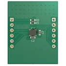
ISM330DLCTR Reference Design
1) PurposeThis project is a small 6-axis IMU breakout/reference design built around the IC1, exposing its main digital interfaces and support pins on headers, with the surrounding passives recommended for a basic 3.3 V I2C implementation. I’m describing the design as it currently exists, not an idealized version, consistent with the project-explanation method .
The board’s purpose is to make the IC1 easy to power, connect, and evaluate.
Functionally, it does three things:
- Powers the IMU from a 3.3 V rail
- Provides the main host interface for communication
- Breaks out additional pins for interrupts and auxiliary interface access
From the datasheet, the sensor itself is a 6-axis IMU combining:
- A 3-axis accelerometer
- A 3-axis gyroscope
It supports:
- I2C or SPI as the main host interface
- An auxiliary interface for external/secondary sensor access or special modes
- Two interrupt outputs
- Industrial-oriented use cases like motion sensing, robotics, vibration monitoring, and navigation
- IC1
- STMicroelectronics 6-axis IMU
- Main chip in the design
- Powered by VDD and VDDIO
- Exposes:
- SCL/SDA for main I2C
- CS for SPI/I2C selection
- INT1/INT2 interrupt outputs
- SCx/SDx/OCS_Aux/SDO_Aux for auxiliary interface features
Both are 100 nF capacitors. This matches the datasheet recommendation for local decoupling on the supply pins.
Both are 10 kΩ resistors. In this design they act as the I2C pull-ups.
Connectors
These two 1x6 headers break out the sensor’s power and signal pins to the outside world.
3) How the Components Interact
Power
The 3.3 V rail feeds:
The decoupling capacitors:
are connected between supply and ground, stabilizing the local power seen by the IMU.
Main communication path
The main digital bus is set up as I2C:
This matches the datasheet guidance that CS tied high selects I2C mode, and that typical I2C configurations use pull-ups.
Mode selection
This is an interesting design choice:
- It does not hard-force one mode on-board
- Instead, it leaves the host or test setup free to decide how to drive the mode-select pin
That makes the board more flexible for evaluation.
Interrupts
These let a host processor receive motion/event notifications without polling continuously.
Auxiliary interface breakout
The design also exposes the auxiliary pins:
This suggests the board is intended not just as a minimal breakout, but as a reference/evaluation platform that exposes more of the chip’s advanced interface options.
4) Design Breakdown
Architecture
This is a very simple architecture:
Power input -> decoupling + pull-ups -> IC1 -> headers for host connection
There is no onboard MCU, regulator, or level shifting. That means the board is intended to be:
- A sensor daughterboard
- A reference circuit
- A development/evaluation subassembly
The implementation is intentionally minimal:
Good choices
- Two 100 nF decoupling capacitors:
- aligns with datasheet guidance
- appropriate for the separate supply domains
- 10 kΩ I2C pull-ups:
- common and safe for low-speed/moderate-speed I2C
- low component count
- Headers on both sides:
- easy lab access
- easy jumper-wire integration
- Breakout of interrupts and auxiliary pins:
- makes more features accessible
- increases usefulness for experimentation
-
Flexibility vs simplicity
- Exposing more pins makes the board more versatile
- But it also makes the design slightly less beginner-proof, because unused lines may need deliberate handling in a final system
-
Minimal BOM vs robustness
- Very small BOM: just sensor, 2 resistors, 2 capacitors, 2 headers
- But no onboard protection, no regulator, and no level translation
-
Generic pull-up value vs performance optimization
- 10 kΩ is simple and broadly usable
- But it is not necessarily optimal for every bus capacitance or speed target
The PCB is already laid out as a compact 2-layer board.
Layout observations
- Board size is about 24 mm x 30 mm
- Only 7 placed components
- Density is low, so routing space is generous
- All airwires are resolved
- ERC checks for floating pins, missing power, and undriven nets are currently clean
That suggests this is a tidy, low-complexity reference layout rather than a dense production module.
6) Key Technologies and Dependencies
Technologies
- MEMS inertial sensing
- I2C / SPI digital interfacing
- Interrupt-driven host integration
- Basic power decoupling
- 2-layer PCB implementation
To actually use this board in a system, you still need:
- An external 3.3 V supply
- An external host MCU/processor
- Firmware that can configure and read the IC1
- Correct handling of CS, SDA/SCL, and optional interrupt/aux pins
In a real system, the flow is roughly:
- Apply 3.3 V and ground
- Pull CS high for I2C operation, or configure for SPI if desired
- Host communicates with IC1 over SDA/SCL
- Sensor measures:
- acceleration
- angular rate
- Optional:
- use INT1/INT2 for event-driven signaling
- use auxiliary pins for advanced modes or external sensor integration
- Pull-up strength
- 10 kΩ is fine for many setups
- If cable length or bus capacitance rises, edges may become too slow
- Power quality
- IMUs are sensitive to supply noise
- Local decoupling helps, but system-level supply cleanliness still matters
- Logic-level compatibility
- The board expects a compatible I/O voltage domain
- If the host is not 3.3 V-compatible, extra circuitry may be required
From the datasheet, the chip supports:
- accelerometer ranges up to ±16 g
- gyro ranges up to ±2000 dps
- low-power and higher-performance operating modes
Actual application performance will depend heavily on:
- mechanical mounting
- vibration environment
- firmware filtering
- calibration
- sampling configuration
Because this is a compact sensor board:
- placement of decoupling near the IMU matters
- ground return quality matters
- mechanical coupling to the measured system matters
- Selecting the correct I2C/SPI mode
- Managing the CS pin correctly
- Choosing appropriate I2C pull-up strength
- Interpreting interrupt behavior correctly
- Making use of auxiliary pins without extra firmware complexity
- Long wires to the headers can degrade I2C integrity
- No onboard regulator means supply quality is the host system’s responsibility
- No explicit protection means lab misuse is easier:
- wrong voltage
- ESD
- accidental wiring mistakes
This kind of board fits well in:
- robotics prototypes
- motion-tracking demos
- vibration monitoring experiments
- industrial sensing evaluation
- drone or stabilization prototyping
- embedded firmware bring-up for IMU drivers
It is especially useful when you want to validate the IC1 before integrating it into a larger custom board.
11) Areas for Improvement
If you wanted to evolve this from a reference design into a more deployment-ready module, good improvements would be:
Electrical robustness
- Add ESD protection on header-exposed lines
- Add clearer/default biasing for CS if I2C-only use is intended
- Optionally add a small onboard 3.3 V regulator if broader supply compatibility is needed
- Add silk labels for pin purpose and orientation
- Consider a single standardized connector instead of two generic headers
- Add configurable solder-jumper options for:
- interface mode
- address/config behavior
- interrupt routing
- Make pull-up values configurable
- Consider stronger pull-ups for faster I2C use cases
- Add test pads for debug and validation
- Add mounting holes or better mechanical definition if this becomes a deployable sensor node
- Improve environmental/mechanical integration for vibration-sensitive applications
This is a clean, minimal, sensible IMU reference design.
What it does well
- Uses the core support parts the datasheet expects
- Exposes the important interfaces
- Keeps the circuit simple and easy to understand
- Provides a practical bridge between the sensor IC and an external host
- It is not a full standalone sensor module
- It is not a protected industrial interface board
- It is not a complete embedded system by itself
So the best way to think about it is:
a bring-up and integration reference board for the IC1, optimized for simplicity, accessibility, and evaluation rather than maximum ruggedness or feature completeness.
If you want, I can also turn this into:
- a block-diagram view
- a pin-by-pin walkthrough
- or a “how to use it with a microcontroller” explanation.
Inspect project schematic
Review BOM too
Check design issues


Welcome 👋
Flux helps you build PCBs faster with an AI teammate!
Create your account to collaborate, stay updated, fork your own version, and get instant answers from our AI agent.