USB 3.1 Interface Project Overview
1:13
Below is an overview of the project as it currently stands:
Project Purpose
The design targets a USB 3.1 interface solution using the FUSB302BMPX device from onsemi. The chip is intended to serve as a USB Type‑C configuration channel controller for high‑speed USB 3.1 applications while keeping the board area very compact (using a 14‑MLP package with a 2.5 × 2.5 mm footprint).
Core Components
-
FUSB302BMPX Controller
- Acts as the brain of the USB interface, handling Type‑C detection, orientation sensing, and configuration channel (CC) negotiation.
- Key dependencies include the precise routing of high‐speed signals and strict adherence to USB 3.1 specifications.
-
Terminal Connections
- Several Terminal parts are deployed to represent the various power and signal nodes on the controller. These include connections for:
- Power Supplies: VDD, VBUS, etc.
- Control and Communication: CC1, CC2, INT_N, SCL, SDA.
- Grounds and Special Signals: GND, EPAD, VCONN.
- These terminal elements serve as interconnection points for external wiring and interface to the eventual USB connector.
- Several Terminal parts are deployed to represent the various power and signal nodes on the controller. These include connections for:
Design & Implementation Breakdown
-
Schematic Creation
- The schematic defines the interconnection of the FUSB302BMPX along with a set of terminal components for all power, ground, and control signals.
- Each terminal is placed with explicit designators (for example, VDD, GND, CC1, CC2) to clearly mark the various signals reviewed in the datasheet.
-
Signal Routing and Interactions
- The device’s CC outputs are interfaced through dedicated terminal symbols to facilitate proper negotiation of cable orientation.
- Power rails (VDD and VBUS) and their associated decoupling strategies are outlined through specific nodes, ensuring power integrity.
- Control signals like INT_N, SCL, and SDA are intended to support communication functions or management of on‑chip functions.
-
PCB Layout Considerations
- The footprint of the FUSB302BMPX demands careful component placement. Although the current project focuses on the schematic connectivity, the layout process will have to address high‑speed routing and impedance control for USB signals.
- Special consideration will be required for differential signal pairs and minimizing loop areas around high‑frequency traces.
-
Key Design Technologies and Dependencies
- USB 3.1 Protocol: Ensures high data rates and proper interfacing for the Type‑C connector.
- Compact Packaging: The use of a 14‑MLP package maximizes space efficiency, which is critical for portable or space‑constrained designs.
- ESD and Signal Protection: Although not yet fully implemented, the design will eventually need strategies to address any vulnerabilities in the high‑speed interface.
Design Choices, Trade-offs, and Optimizations
-
Compact Footprint versus Routing Complexity:
The decision to use a 2.5 × 2.5 mm package minimizes board space but brings challenges in layout—particularly regarding trace impedance control and heat dissipation. -
Use of Terminal Symbols for Flexibility:
By breaking down the connections into separate terminal parts, the design remains modular and easier to adjust. This approach supports iterative optimization as additional passive or protective components are introduced later in the design cycle. -
Performance Considerations:
- Signal Integrity: Ensuring that high‑speed signals adhere to USB 3.1 specifications will be critical. This may require refinements in pad design, trace length matching, and careful dielectric material selection.
- Thermal Management: With a compact design, thermal dissipation may be limited. Trade-offs between component density and sufficient cooling must be assessed.
Potential Challenges and Areas for Future Enhancement
-
Challenges:
- High‑Speed Signal Routing: As USB 3.1 protocols are sensitive to impedance mismatches and trace discontinuities, accurate PCB layout and verification of differential pair routing will be essential.
- Thermal Constraints: The compact size might elevate operating temperatures. Future iterations may require additional thermal strategy improvements.
- Protocol Compliance: Ensuring strict compliance with USB Type‑C and USB 3.1 standards might involve additional components (such as filtering networks or protection circuits) not yet integrated.
-
Future Enhancements:
- Integration of Protective Elements: Incorporating ESD protection, decoupling capacitors per power pin, and current‐limiting resistors can help enhance reliability.
- Layout Optimization: Advanced PCB routing techniques should be applied to minimize electromagnetic interference (EMI) and ensure signal integrity.
- Scalability: Once the core USB interface is validated, consider adding support for additional features (such as power delivery negotiation or advanced debugging interfaces) to extend the design’s utility.
- Design Verification: Future iterations will likely involve refined DRC (Design Rule Check) reviews to address any potential mismatches or errors in the schematic and layout.
Real‑World Applications
-
USB Type‑C Devices:
The design is primed for integration into devices that require modern USB Type‑C connectivity, such as smartphones, tablets, or peripheral devices with high‑speed data transfer capabilities. -
Compact Embedded Systems:
Its small footprint makes it ideal for embedded systems where space is at a premium without sacrificing USB performance. -
High‑Speed Data Applications:
With USB 3.1 support, the controller is suited for high‑data‑rate applications including high‑resolution imaging, data storage interfaces, and video streaming devices.
This overview captures the current design focus, technology choices, and potential areas for ongoing improvements. Each stage of the project—from schematic connectivity through layout challenges—is critical to delivering a robust, high‑performance USB interface solution.
Next component selection
Identify passive components
Explore further options
404 days
Ready.
VCONN
EPAD
VDD
CC2
VBUS
INT_N
VCONN
SCL
CC2
CC1
GND
VDD
SDA
CC1
GND
Reviews

- Wirelessly connects nets on schematic. Used to organize schematics and separate functional blocks. To wirelessly connect net portals, give them same designator. #portaljharwinbarrozo43.0M
- Wirelessly connects power nets on schematic. Identical to the net portal, but with a power symbol. Used to organize schematics and separate functional blocks. To wirelessly connect power net portals, give them the same designator. #portal #powerjharwinbarrozo11.4M
- A generic fixed resistor ideal for rapid circuit topology development. Its footprint automatically adapts based on the selected package case code—supporting 0402, 0603, 0805, 1203, and many other standard SMD packages, as well as axial horizontal and vertical configurations. Save precious design time by seamlessly add more information to this part (value, footprint, etc.) as it becomes available. Standard resistor values: 1.0 ohm, 10 ohm, 100 ohm, 1.0k ohm, 10k ohm, 100k ohm, 1.0M ohm 1.1 ohm, 11 ohm, 110 ohm, 1.1k ohm, 11k ohm, 110k ohm, 1.1M ohm 1.2 ohm, 12 ohm, 120 ohm, 1.2k ohm, 12k ohm, 120k ohm, 1.2M ohm 1.3 ohm, 13 ohm, 130 ohm, 1.3k ohm, 13k ohm, 130k ohm, 1.3M ohm 1.5 ohm, 15 ohm, 150 ohm, 1.5k ohm, 15k ohm, 150k ohm, 1.5M ohm 1.6 ohm, 16 ohm, 160 ohm, 1.6k ohm, 16k ohm, 160k ohm, 1.6M ohm 1.8 ohm, 18 ohm, 180 ohm, 1.8K ohm, 18k ohm, 180k ohm, 1.8M ohm 2.0 ohm, 20 ohm, 200 ohm, 2.0k ohm, 20k ohm, 200k ohm, 2.0M ohm 2.2 ohm, 22 ohm, 220 ohm, 2.2k ohm, 22k ohm, 220k ohm, 2.2M ohm 2.4 ohm, 24 ohm, 240 ohm, 2.4k ohm, 24k ohm, 240k ohm, 2.4M ohm 2.7 ohm, 27 ohm, 270 ohm, 2.7k ohm, 27k ohm, 270k ohm, 2.7M ohm 3.0 ohm, 30 ohm, 300 ohm, 3.0K ohm, 30K ohm, 300K ohm, 3.0M ohm 3.3 ohm, 33 ohm, 330 ohm, 3.3k ohm, 33k ohm, 330k ohm, 3.3M ohm 3.6 ohm, 36 ohm, 360 ohm, 3.6k ohm, 36k ohm, 360k ohm, 3.6M ohm 3.9 ohm, 39 ohm, 390 ohm, 3.9k ohm, 39k ohm, 390k ohm, 3.9M ohm 4.3 ohm, 43 ohm, 430 ohm, 4.3k ohm, 43K ohm, 430K ohm, 4.3M ohm 4.7 ohm, 47 ohm, 470 ohm, 4.7k ohm, 47k ohm, 470k ohm, 4.7M ohm 5.1 ohm, 51 ohm, 510 ohm, 5.1k ohm, 51k ohm, 510k ohm, 5.1M ohm 5.6 ohm, 56 ohm, 560 ohm, 5.6k ohm, 56k ohm, 560k ohm, 5.6M ohm 6.2 ohm, 62 ohm, 620 ohm, 6.2k ohm, 62K ohm, 620K ohm, 6.2M ohm 6.8 ohm, 68 ohm, 680 ohm, 6.8k ohm, 68k ohm, 680k ohm, 6.8M ohm 7.5 ohm, 75 ohm, 750 ohm, 7.5k ohm, 75k ohm, 750k ohm, 7.5M ohm 8.2 ohm, 82 ohm, 820 ohm, 8.2k ohm, 82k ohm, 820k ohm, 8.2M ohm 9.1 ohm, 91 ohm, 910 ohm, 9.1k ohm, 91k ohm, 910k ohm, 9.1M ohm #generics #CommonPartsLibraryjharwinbarrozo1.5M
- A generic fixed capacitor ideal for rapid circuit topology development. You can choose between polarized and non-polarized types, its symbol and the footprint will automatically adapt based on your selection. Supported options include standard SMD sizes for ceramic capacitors (e.g., 0402, 0603, 0805), SMD sizes for aluminum electrolytic capacitors, and through-hole footprints for polarized capacitors. Save precious design time by seamlessly add more information to this part (value, footprint, etc.) as it becomes available. Standard capacitor values: 1.0pF, 10pF, 100pF, 1000pF, 0.01uF, 0.1uF, 1.0uF, 10uF, 100uF, 1000uF, 10000uF 1.1pF, 11pF, 110pF, 1100pF 1.2pF, 12pF, 120pF, 1200pF 1.3pF, 13pF, 130pF, 1300pF 1.5pF, 15pF, 150pF, 1500pF, 0.015uF, 0.15uF, 1.5uF, 15uF, 150uF, 1500uF 1.6pF, 16pF, 160pF, 1600pF 1.8pF, 18pF, 180pF, 1800pF 2.0pF, 20pF, 200pF, 2000pF 2.2pF, 22pF, 220pF, 2200pF, 0.022uF, 0.22uF, 2.2uF, 22uF, 220uF, 2200uF 2.4pF, 24pF, 240pF, 2400pF 2.7pF, 27pF, 270pF, 2700pF 3.0pF, 30pF, 300pF, 3000pF 3.3pF, 33pF, 330pF, 3300pF, 0.033uF, 0.33uF, 3.3uF, 33uF, 330uF, 3300uF 3.6pF, 36pF, 360pF, 3600pF 3.9pF, 39pF, 390pF, 3900pF 4.3pF, 43pF, 430pF, 4300pF 4.7pF, 47pF, 470pF, 4700pF, 0.047uF, 0.47uF, 4.7uF, 47uF, 470uF, 4700uF 5.1pF, 51pF, 510pF, 5100pF 5.6pF, 56pF, 560pF, 5600pF 6.2pF, 62pF, 620pF, 6200pF 6.8pF, 68pF, 680pF, 6800pF, 0.068uF, 0.68uF, 6.8uF, 68uF, 680uF, 6800uF 7.5pF, 75pF, 750pF, 7500pF 8.2pF, 82pF, 820pF, 8200pF 9.1pF, 91pF, 910pF, 9100pF #generics #CommonPartsLibraryjharwinbarrozo1.5M
- A generic fixed inductor suitable for rapid circuit topology development. The footprint automatically adapts based on the selected package, supporting standard SMD sizes (e.g., 0402, 0603, 0805) as well as well-known inductor packages such as SDR1806, PA4320, SRN6028, and SRR1260. Standard inductor values: 1.0 nH, 10 nH, 100 nH, 1.0 µH, 10 µH, 100 µH, 1.0 mH 1.2 nH, 12 nH, 120 nH, 1.2 µH, 12 µH, 120 µH, 1.2 mH 1.5 nH, 15 nH, 150 nH, 1.5 µH, 15 µH, 150 µH, 1.5 mH 1.8 nH, 18 nH, 180 nH, 1.8 µH, 18 µH, 180 µH, 1.8 mH 2.2 nH, 22 nH, 220 nH, 2.2 µH, 22 µH, 220 µH, 2.2 mH 2.7 nH, 27 nH, 270 nH, 2.7 µH, 27 µH, 270 µH, 2.7 mH 3.3 nH, 33 nH, 330 nH, 3.3 µH, 33 µH, 330 µH, 3.3 mH 3.9 nH, 39 nH, 390 nH, 3.9 µH, 39 µH, 390 µH, 3.9 mH 4.7 nH, 47 nH, 470 nH, 4.7 µH, 47 µH, 470 µH, 4.7 mH 5.6 nH, 56 nH, 560 nH, 5.6 µH, 56 µH, 560 µH, 5.6 mH 6.8 nH, 68 nH, 680 nH, 6.8 µH, 68 µH, 680 µH, 6.8 mH 8.2 nH, 82 nH, 820 nH, 8.2 µH, 82 µH, 820 µH, 8.2 mH #generics #CommonPartsLibraryjharwinbarrozo15.7k
- An electrical connector acting as reusable interface to a conductor and creating a point where external circuits can be connected.Terminal
- 47 kOhms ±5% 0.125W, 1/8W Chip Resistor 0805 (2012 Metric) Automotive AEC-Q200 Thick Film #forLedBlinkjharwinbarrozo1.2M
- 10uF Capacitor Aluminum Polymer 20% 16V SMD 5x5.3mm #forLedBlink #commonpartslibrary #capacitor #aluminumpolymer #radialcanjharwinbarrozo1.2M
- Yellow 595nm LED Indication - Discrete 1.7V 1206 (3216 Metric) #forLedBlinkjharwinbarrozo1.1M


FUSB302BMPX
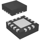
USB Controller USB 3.1 USB Interface 14-MLP (2.5x2.5)
Properties
Integrated Circuit
onsemi
FUSB302BMPX
U
Parametric
Pricing & Availability
Distributor | Qty 1 |
|---|
Controls
Welcome 👋
Flux accelerates your PCB design with AI.
Create your account to start using this component and bring your ideas to life.