Copper Pour for GND Connections

2:06

Reviewing ground fill process.

Clarifying tool usage for instructions.

Defining tool priorities for guidance.

Clarifying instructions on ground fills.

Accessing knowledge base.

Reading docs about How to enable or show ground fill on the bottom layer only, assign it to GND, configure via stitching, and re-pour in Flux PCB layout. Also how to toggle visibility of copper fills..

Preparing for user instructions.

Here’s what the Flux documentation says about enabling a GND copper fill on a specific layer and adding via stitching:
Image

Image

“Fills can be enabled or disabled on each layer by assigning a "Connected Layers" rule to the target net. If the target net is a ground net it is known as a ground fill, while if the target net is a power net it's known as a power fill.
To enable or disable a copper fill for a target net:
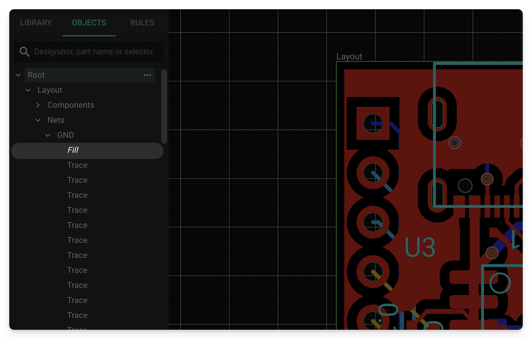
  • Select the target net (nested under Root → Layout → Nets in the Objects panel
  • Add a "Connected Layers" rule from the "object-specific rules" menu on the right.
  • Select all layers for which you want the fill to be enabled. Leaving the text box empty will disable the fill connected to that net on every layer.
Info Leaving the "Connected Layers" rule empty will disable copper fills on every layer for that net.”
“Via stitching can be enabled and configured with the use of two rules:
  • Fill Stitching Density: vias will be spaced by the amount specified in this rule. Any non-zero value enables via stitching.
  • Fill Stitching Offset: shifts the via stitching block by the amount specified.
Follow these steps to add one or both of the rules:
  • Select the ground net (nested under Layout → Nets → GND in the Objects panel)
  • Add the desired rule from the "object-specific rules" menu on the right.
  • Enter the offset and/or density values as distances.
Note: both rules accept x and y input (vector rules). For example, typing "10mm 13mm" on Fill Density will create stitching with 10mm separation on the x-axis and 13mm separation on the y-axis.” Source
Would you like me to stay with you while you add:
  • Connected Layers = Bottom (for GND), and
  • Fill Stitching Density (your chosen spacing) on GND?
Bottom-only GND fill
Choose stitching spacing
Fix floating copper
Adjust fill clearances
Split grounds for shield
79 days

J6 CC1 - R1 1
J6 CC1 - R1 1
J6 CC2 - R2 1
SW1 P3 - U1 5V
J6 CC2 - R2 1
GND
SW2
J6
Type-C-2.0-6Pin


  • Ground
    A common return path for electric current. Commonly known as ground.
  • Net Portal
    Wirelessly connects nets on schematic. Used to organize schematics and separate functional blocks. To wirelessly connect net portals, give them same designator. #portal
  • Power Net Portal
    Wirelessly connects power nets on schematic. Identical to the net portal, but with a power symbol. Used to organize schematics and separate functional blocks. To wirelessly connect power net portals, give them the same designator. #portal #power
  • Generic Resistor
    A generic fixed resistor ideal for rapid circuit topology development. Its footprint automatically adapts based on the selected package case code—supporting 0402, 0603, 0805, 1203, and many other standard SMD packages, as well as axial horizontal and vertical configurations. Save precious design time by seamlessly add more information to this part (value, footprint, etc.) as it becomes available. Standard resistor values: 1.0 ohm, 10 ohm, 100 ohm, 1.0k ohm, 10k ohm, 100k ohm, 1.0M ohm 1.1 ohm, 11 ohm, 110 ohm, 1.1k ohm, 11k ohm, 110k ohm, 1.1M ohm 1.2 ohm, 12 ohm, 120 ohm, 1.2k ohm, 12k ohm, 120k ohm, 1.2M ohm 1.3 ohm, 13 ohm, 130 ohm, 1.3k ohm, 13k ohm, 130k ohm, 1.3M ohm 1.5 ohm, 15 ohm, 150 ohm, 1.5k ohm, 15k ohm, 150k ohm, 1.5M ohm 1.6 ohm, 16 ohm, 160 ohm, 1.6k ohm, 16k ohm, 160k ohm, 1.6M ohm 1.8 ohm, 18 ohm, 180 ohm, 1.8K ohm, 18k ohm, 180k ohm, 1.8M ohm 2.0 ohm, 20 ohm, 200 ohm, 2.0k ohm, 20k ohm, 200k ohm, 2.0M ohm 2.2 ohm, 22 ohm, 220 ohm, 2.2k ohm, 22k ohm, 220k ohm, 2.2M ohm 2.4 ohm, 24 ohm, 240 ohm, 2.4k ohm, 24k ohm, 240k ohm, 2.4M ohm 2.7 ohm, 27 ohm, 270 ohm, 2.7k ohm, 27k ohm, 270k ohm, 2.7M ohm 3.0 ohm, 30 ohm, 300 ohm, 3.0K ohm, 30K ohm, 300K ohm, 3.0M ohm 3.3 ohm, 33 ohm, 330 ohm, 3.3k ohm, 33k ohm, 330k ohm, 3.3M ohm 3.6 ohm, 36 ohm, 360 ohm, 3.6k ohm, 36k ohm, 360k ohm, 3.6M ohm 3.9 ohm, 39 ohm, 390 ohm, 3.9k ohm, 39k ohm, 390k ohm, 3.9M ohm 4.3 ohm, 43 ohm, 430 ohm, 4.3k ohm, 43K ohm, 430K ohm, 4.3M ohm 4.7 ohm, 47 ohm, 470 ohm, 4.7k ohm, 47k ohm, 470k ohm, 4.7M ohm 5.1 ohm, 51 ohm, 510 ohm, 5.1k ohm, 51k ohm, 510k ohm, 5.1M ohm 5.6 ohm, 56 ohm, 560 ohm, 5.6k ohm, 56k ohm, 560k ohm, 5.6M ohm 6.2 ohm, 62 ohm, 620 ohm, 6.2k ohm, 62K ohm, 620K ohm, 6.2M ohm 6.8 ohm, 68 ohm, 680 ohm, 6.8k ohm, 68k ohm, 680k ohm, 6.8M ohm 7.5 ohm, 75 ohm, 750 ohm, 7.5k ohm, 75k ohm, 750k ohm, 7.5M ohm 8.2 ohm, 82 ohm, 820 ohm, 8.2k ohm, 82k ohm, 820k ohm, 8.2M ohm 9.1 ohm, 91 ohm, 910 ohm, 9.1k ohm, 91k ohm, 910k ohm, 9.1M ohm #generics #CommonPartsLibrary
  • Generic Capacitor
    A generic fixed capacitor ideal for rapid circuit topology development. You can choose between polarized and non-polarized types, its symbol and the footprint will automatically adapt based on your selection. Supported options include standard SMD sizes for ceramic capacitors (e.g., 0402, 0603, 0805), SMD sizes for aluminum electrolytic capacitors, and through-hole footprints for polarized capacitors. Save precious design time by seamlessly add more information to this part (value, footprint, etc.) as it becomes available. Standard capacitor values: 1.0pF, 10pF, 100pF, 1000pF, 0.01uF, 0.1uF, 1.0uF, 10uF, 100uF, 1000uF, 10000uF 1.1pF, 11pF, 110pF, 1100pF 1.2pF, 12pF, 120pF, 1200pF 1.3pF, 13pF, 130pF, 1300pF 1.5pF, 15pF, 150pF, 1500pF, 0.015uF, 0.15uF, 1.5uF, 15uF, 150uF, 1500uF 1.6pF, 16pF, 160pF, 1600pF 1.8pF, 18pF, 180pF, 1800pF 2.0pF, 20pF, 200pF, 2000pF 2.2pF, 22pF, 220pF, 2200pF, 0.022uF, 0.22uF, 2.2uF, 22uF, 220uF, 2200uF 2.4pF, 24pF, 240pF, 2400pF 2.7pF, 27pF, 270pF, 2700pF 3.0pF, 30pF, 300pF, 3000pF 3.3pF, 33pF, 330pF, 3300pF, 0.033uF, 0.33uF, 3.3uF, 33uF, 330uF, 3300uF 3.6pF, 36pF, 360pF, 3600pF 3.9pF, 39pF, 390pF, 3900pF 4.3pF, 43pF, 430pF, 4300pF 4.7pF, 47pF, 470pF, 4700pF, 0.047uF, 0.47uF, 4.7uF, 47uF, 470uF, 4700uF 5.1pF, 51pF, 510pF, 5100pF 5.6pF, 56pF, 560pF, 5600pF 6.2pF, 62pF, 620pF, 6200pF 6.8pF, 68pF, 680pF, 6800pF, 0.068uF, 0.68uF, 6.8uF, 68uF, 680uF, 6800uF 7.5pF, 75pF, 750pF, 7500pF 8.2pF, 82pF, 820pF, 8200pF 9.1pF, 91pF, 910pF, 9100pF #generics #CommonPartsLibrary
  • Generic Inductor
    A generic fixed inductor suitable for rapid circuit topology development. The footprint automatically adapts based on the selected package, supporting standard SMD sizes (e.g., 0402, 0603, 0805) as well as well-known inductor packages such as SDR1806, PA4320, SRN6028, and SRR1260. Standard inductor values: 1.0 nH, 10 nH, 100 nH, 1.0 µH, 10 µH, 100 µH, 1.0 mH 1.2 nH, 12 nH, 120 nH, 1.2 µH, 12 µH, 120 µH, 1.2 mH 1.5 nH, 15 nH, 150 nH, 1.5 µH, 15 µH, 150 µH, 1.5 mH 1.8 nH, 18 nH, 180 nH, 1.8 µH, 18 µH, 180 µH, 1.8 mH 2.2 nH, 22 nH, 220 nH, 2.2 µH, 22 µH, 220 µH, 2.2 mH 2.7 nH, 27 nH, 270 nH, 2.7 µH, 27 µH, 270 µH, 2.7 mH 3.3 nH, 33 nH, 330 nH, 3.3 µH, 33 µH, 330 µH, 3.3 mH 3.9 nH, 39 nH, 390 nH, 3.9 µH, 39 µH, 390 µH, 3.9 mH 4.7 nH, 47 nH, 470 nH, 4.7 µH, 47 µH, 470 µH, 4.7 mH 5.6 nH, 56 nH, 560 nH, 5.6 µH, 56 µH, 560 µH, 5.6 mH 6.8 nH, 68 nH, 680 nH, 6.8 µH, 68 µH, 680 µH, 6.8 mH 8.2 nH, 82 nH, 820 nH, 8.2 µH, 82 µH, 820 µH, 8.2 mH #generics #CommonPartsLibrary
  • Terminal
    Terminal
    An electrical connector acting as reusable interface to a conductor and creating a point where external circuits can be connected.
  • RMCF0805JT47K0
    47 kOhms ±5% 0.125W, 1/8W Chip Resistor 0805 (2012 Metric) Automotive AEC-Q200 Thick Film #forLedBlink
  • 875105359001
    10uF Capacitor Aluminum Polymer 20% 16V SMD 5x5.3mm #forLedBlink #commonpartslibrary #capacitor #aluminumpolymer #radialcan
  • CTL1206FYW1T
    Yellow 595nm LED Indication - Discrete 1.7V 1206 (3216 Metric) #forLedBlink

Jiji

Jiji thumbnail
ESP32-S3 CAM Audio-Visual Controller with I2S MEMS Microphone, Class-D Amplifier, SPI Display, Servos, Capacitive Touch and Integrated USB-C Power-Only Sink (VBUS via J6 → 5V_IN → SW1:P1 → 5V_SW, CC1/CC2 5.1 kΩ to GND, VBUS TVS Surge Protection) #USB_C #PowerManagement #5V

Properties

Diagram


"J6 VBUS" "5V_IN" "J6 VBUS__1" "SW1:P1" "5V_SW" "Existing node_5V consumers" "J6 CC1" "R_CC1 5.1k" "J6 CC2" "R_CC2 5.1k" "GND" "VBUS TVS diode"

Pricing & Availability

Distributor

Qty 1

LCSC

$0.32–$0.43

Controls