Timers and RTCs
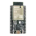
ESP32-C3-MINI-1-N4
The ESP32-C3-MINI-1-N4 is a compact, low-power wireless module from Espressif Systems built around the ESP32-C3 SoC. It integrates a 32-bit RISC-V single-core processor, 2.4 GHz Wi-Fi, Bluetooth 5 Low Energy (BLE), onboard flash memory, crystal oscillator, RF circuitry, and PCB antenna in a small surface-mount package. The module is designed for IoT devices, smart home products, industrial automation, sensor nodes, wearable devices, and other wireless embedded applications. Key Features 32-bit RISC-V Single-Core CPU Up to 160 MHz operating frequency Optimized for low-power IoT applications Integrated Memory 4 MB embedded Flash (N4 version) 400 KB SRAM 384 KB ROM 8 KB RTC SRAM Wireless Connectivity IEEE 802.11 b/g/n Wi-Fi (2.4 GHz) Data rates up to 150 Mbps Bluetooth 5 LE support Bluetooth Mesh capability Simultaneous Wi-Fi and Bluetooth operation using a shared antenna Security Features Secure Boot Flash Encryption Hardware cryptographic acceleration RSA, AES, HMAC, and Digital Signature support Rich Peripheral Set Up to 15 GPIOs UART SPI I²C I²S USB Serial/JTAG PWM TWAI (CAN 2.0 compatible) SAR ADC Timers and Watchdog timers Temperature sensor Integrated Components On-board PCB antenna 40 MHz crystal oscillator RF matching circuitry No external RF design required Power Supply Operating voltage: 3.0 V to 3.6 V Designed for low-power applications Environmental Specifications Operating temperature: −40°C to +85°C (N4 variant) RoHS and REACH compliant #module #RF-Transceiver #ESP32-C3
130 Uses
0 Stars
ESP32-DevKitC
The ESP32-DevKitC is an official ESP32-based development board from Espressif Systems designed for rapid prototyping and IoT application development. It integrates an ESP32 module (such as ESP32-WROOM-32E or ESP32-WROVER variants), USB-to-UART programming interface, power regulation circuitry, reset and boot buttons, and access to most ESP32 GPIOs through dual-row headers. The board is breadboard-friendly and supports wireless connectivity, making it suitable for smart devices, industrial monitoring, home automation, wearable electronics, and embedded control systems. Key Features ESP32 Dual-Core Processor Xtensa® 32-bit LX6 dual-core MCU Up to 240 MHz clock frequency High-performance embedded processing capability. Wireless Connectivity Integrated 2.4 GHz Wi-Fi (802.11 b/g/n) Bluetooth Classic (BR/EDR) and Bluetooth Low Energy (BLE) support. Memory Typically includes 4 MB SPI Flash Some variants provide additional PSRAM for memory-intensive applications. Rich Peripheral Interfaces UART, SPI, I²C, I²S, SDIO ADC and DAC PWM outputs Capacitive touch sensing Pulse counter and timer peripherals. Extensive GPIO Access Most ESP32 pins are broken out to headers Supports digital I/O, interrupts, analog inputs, and communication interfaces. Development-Friendly Hardware USB-to-UART bridge for programming and debugging Dedicated EN (Reset) and BOOT buttons On-board 3.3 V regulator Breadboard-compatible layout. Flexible Power Options Powered through Micro-USB and onboard power circuitry Supports external power connections through header pins. #DevelopmentBoard
176 Uses
0 Stars
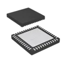
NRF52832-QFAA-R7
IC RF TxRx + MCU Bluetooth Bluetooth v5.3 2.4GHz 48-VFQFN Exposed Pad NRF52832-QFAA-R7 is an ultra-low-power wireless System-on-Chip (SoC) from Nordic Semiconductor, designed for Bluetooth Low Energy (BLE), ANT, NFC, and proprietary 2.4 GHz wireless applications. It integrates a high-performance ARM Cortex-M4F processor, memory, peripherals, and a 2.4 GHz radio into a single chip, making it ideal for IoT devices, wearables, wireless sensors, beacons, and smart peripherals. GHz protocols • 2.4 GHz transceiver • -96 dBm sensitivity in Bluetooth® low energy mode • Supported data rates: 1 Mbps, 2 Mbps Bluetooth® low energy mode • -20 to +4 dBm TX power, configurable in 4 dB steps • On-chip balun (single-ended RF) • 5.3 mA peak current in TX (0 dBm) • 5.4 mA peak current in RX • RSSI (1 dB resolution) • ARM® Cortex®-M4 32-bit processor with FPU, 64 MHz • 215 EEMBC CoreMark® score running from flash memory • 58 μA/MHz running from flash memory • 51.6 μA/MHz running from RAM • Data watchpoint and trace (DWT), embedded trace macrocell (ETM), and instrumentation trace macrocell (ITM) • Serial wire debug (SWD) • Trace port • Flexible power management • 1.7 V–3.6 V supply voltage range • Fully automatic LDO and DC/DC regulator system • Fast wake-up using 64 MHz internal oscillator • 0.3 μA at 3 V in System OFF mode • 0.7 μA at 3 V in System OFF mode with full 64 kB RAM retention • 1.9 μA at 3 V in System ON mode, no RAM retention, wake on RTC • Memory • 512 kB flash/64 kB RAM • 256 kB flash/32 kB RAM • Nordic SoftDevice ready • Support for concurrent multi-protocol • Type 2 near field communication (NFC-A) tag with wakeup-on-field and touchto-pair capabilities • 12-bit, 200 ksps ADC - 8 configurable channels with programmable gain • 64 level comparator • 15 level low power comparator with wakeup from System OFF mode • Temperature sensor • 32 general purpose I/O pins • 3x 4-channel pulse width modulator (PWM) unit with EasyDMA • Digital microphone interface (PDM) • 5x 32-bit timer with counter mode • Up to 3x SPI master/slave with EasyDMA • Up to 2x I2C compatible 2-wire master/slave • I2S with EasyDMA • UART (CTS/RTS) with EasyDMA • Programmable peripheral interconnect (PPI) • Quadrature decoder (QDEC) • AES HW encryption with EasyDMA • Autonomous peripheral operation without CPU intervention using PPI and EasyDMA • 3x real-time counter (RTC) • Single crystal operation • Package variants • QFN48 package, 6 × 6 mm • WLCSP package, 3.0 × 3.2 mm #CommonPartsLibrary #IntegratedCircuit
49 Uses
0 Stars
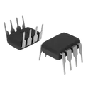
TLC555IP
555 Type, Timer/Oscillator (Single) IC 2.1MHz 8-PDIP The TLC555 is a CMOS monolithic timing circuit. The timer is fully compatible with CMOS, TTL, and MOS logic and operates at frequencies up to 2MHz. Because of a high input impedance, this device supports smaller timing capacitors than those supported by the NE555 or LM555. As a result, more accurate time delays and oscillations are possible. Power consumption is low across the full range of power-supply voltage. • Very low power consumption: – 1mW typical at VDD = 5V • Capable of operation in astable mode • CMOS output capable of swinging rail to rail • High output current capability – Sink: 100mA typical – Source: 10mA typical • Output fully compatible with CMOS, TTL, and MOS • Low supply current reduces spikes during output transitions • Single-supply operation from 2V to 15V • Functionally interchangeable with the NE555; has same pinout • ESD protection exceeds 1000V per ANSI/ESDA/ JEDEC JS-001 • Available in Q-temp automotive – High-reliability automotive applications – Configuration control and print support – Qualification to automotive standards #CommonPartsLibrary #IntegratedCircuit
62 Uses
0 Stars
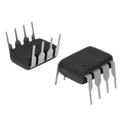
TLC555CP
555 Type, Timer/Oscillator (Single) IC 2.1MHz 8-PDIP Like the NE555, the TLC555 has a trigger level equal to approximately one-third of the supply voltage and a threshold level equal to approximately two-thirds of the supply voltage. These levels can be altered by use of the control voltage terminal (CONT). When the trigger input (TRIG) falls below the trigger level, the flip-flop is set and the output goes high. If TRIG is above the trigger level and the threshold input (THRES) is above the threshold level, the flip-flop is reset and the output is low. The reset input (RESET) can override all other inputs and can be used to initiate a new timing cycle. If RESET is low, the flip-flop is reset and the output is low. Whenever the output is low, a low-impedance path is provided between the discharge terminal (DISCH) and GND. All unused inputs must be tied to an appropriate logic level to prevent false triggering. • Very low power consumption: – 1mW typical at VDD = 5V • Capable of operation in astable mode • CMOS output capable of swinging rail to rail • High output current capability – Sink: 100mA typical – Source: 10mA typical • Output fully compatible with CMOS, TTL, and MOS • Low supply current reduces spikes during output transitions • Single-supply operation from 2V to 15V • Functionally interchangeable with the NE555; has same pinout • ESD protection exceeds 1000V per ANSI/ESDA/ JEDEC JS-001 • Available in Q-temp automotive – High-reliability automotive applications – Configuration control and print support – Qualification to automotive standards #CommonPartsLibrary #IntegratedCircuit
93 Uses
0 Stars
TPS3828-33DBVR
Supervisor Open Drain or Open Collector 1 Channel SOT-23-5 The TPS382x family of supervisors provide circuit initialization and timing supervision, primarily for DSP and processor-based systems. During power on, RESET asserts when the supply voltage VDD becomes greater than 1.1V. Thereafter, the supply voltage supervisor monitors VDD and keeps RESET active low as long as VDD remains less than the threshold voltage, VIT−. An internal timer delays the return of the output to the inactive state (high) to make sure proper system reset. The delay time, td, starts after VDD has risen above the threshold voltage (VIT− + VHYS). When the supply voltage drops below the threshold voltage VIT−, the output becomes active (low) again. No external components are required. All the devices of this family have a fixed-sense threshold voltage, VIT–, set by an internal voltage divider. The TPS382x family also offers watchdog time out options of 200ms (TPS3820) and 1.6s (TPS3823, TPS3824, and TPS3828). • Power-on reset generator with a fixed delay time of 200ms (TPS3823, TPS3824, TPS3825, and TPS3828) or 25ms (TPS3820) • Manual reset input (TPS3820, TPS3823, TPS3825, and TPS3828) • Reset output available in active-low (TPS3820, TPS3823, TPS3824, and TPS3825), active-high (TPS3824 and TPS3825), and open drain (TPS3828) • Supply voltage supervision range: 2.5V, 3V, 3.3V, 5V • Watchdog timer (TPS3820, TPS3823, TPS3824, and TPS3828) • Supply current of 15μA (typical) • 5-pin SOT-23 package • Temperature range: −40°C to 85°C (−40°C to 125°C for TPS3823A-33) #CommonPartsLibrary #IntegratedCircuit #PowerManagement #Supervisor
4 Uses
0 Stars
nRF52810-QCAA-R
IC RF TxRx + MCU Bluetooth Bluetooth v5.0 2.4GHz 32-VFQFN Exposed Pad nRF52810-QCAA-R is a multiprotocol ultra-low-power wireless System-on-Chip from Nordic Semiconductor designed for Bluetooth Low Energy and proprietary wireless communication applications. The device integrates a high-performance ARM Cortex-M processor, radio transceiver, memory resources, and peripheral interfaces into a compact package optimized for low-power embedded systems and IoT devices. This SoC supports reliable wireless connectivity with low energy consumption, making it suitable for wearable electronics, wireless sensors, smart home devices, industrial monitoring systems, and battery-powered portable applications. The integrated radio architecture provides stable RF performance with support for advanced wireless features, secure communication, and efficient coexistence in crowded RF environments. The nRF52810-QCAA-R includes multiple GPIOs, serial communication peripherals, timers, PWM functionality, analog interfaces, and low-power operating modes that simplify embedded hardware design and firmware development. Its compact package and optimized power profile make it ideal for space-constrained and energy-sensitive wireless applications. #commonpartslibrary #nordicsemiconductor #bluetoothlowenergy #wirelesssoc #iotdevices #embeddedhardware #rfdesign #lowpowerdesign #wearableelectronics #wirelesscommunication
68 Uses
0 Stars
BQ24074RGTT
Stand-alone single-cell linear battery charger with power path BQ24074RGTT is a highly integrated standalone linear charger and power-path management IC from Texas Instruments designed for single-cell Li-Ion/Li-Polymer battery-powered portable devices. It supports charging directly from USB ports or external adapters while simultaneously powering the system load through integrated Dynamic Power Path Management (DPPM). The device is commonly used in portable electronics, IoT devices, wireless accessories, handheld medical devices, and battery-powered embedded systems. Key Features Single-cell Li-Ion/Li-Polymer battery charger Up to 1.5 A programmable charge current Integrated Dynamic Power Path Management (DPPM) USB-compliant charging support Selectable 100 mA / 500 mA USB current limits Programmable input current limit up to 1.5 A Supports both USB input and wall adapters Input overvoltage protection up to 28 V absolute maximum Integrated thermal regulation and thermal shutdown Reverse-current and short-circuit protection Programmable pre-charge and fast-charge safety timers Battery temperature monitoring via NTC thermistor input Charge status outputs for charging/done indication Current monitoring output (ISET) Compact 16-pin VQFN (3×3 mm) package Wide operating temperature range suitable for industrial applications Typical Applications TWS charging cases and earbuds Portable medical devices IoT and asset tracking systems Handheld gaming accessories Video doorbells and IP cameras Portable embedded systems and development boards Important Design Notes Designed specifically for 1-cell battery applications Requires proper thermal PCB layout due to linear charging architecture DPPM allows the system to operate even with a deeply discharged or missing battery Recommended for compact designs needing integrated charging and system power-path control #CommonPartsLibrary #IntegratedCircuit #PowerManagement
269 Uses
0 Stars
TPS259474LRPWR
IC SURGE STOPPER 2.7V~23V VQFN-10-HR(2x2) The TPS25947xx family of eFuses is a highly integrated circuit protection and power management solution in a small package. The devices provide multiple protection modes using very few external components and are a robust defense against overloads, short-circuits, voltage surges, reverse polarity and excessive inrush current. With integrated back-to-back FETs, reverse current flow from output to input is blocked at all times, making the devices an excellent choice for power MUX/ORing applications as well as systems which need load side energy hold up storage in case input power supply fails. The devices use linear ORing based scheme to establish an almost zero DC reverse current and emulate ideal diode behavior with minimum forward voltage drop and power dissipation. Output slew rate and inrush current can be adjusted using an external capacitor. Loads are protected from input overvoltage conditions either by clamping the output to a safe fixed maximum voltage (pin selectable), or by cutting off the output if input exceeds an adjustable overvoltage threshold. The devices respond to output overload by actively limiting the current or breaking the circuit. The output current limit threshold as well as the transient overcurrent blanking timer are user adjustable. The current limit control pin also functions as an analog load current monitor. The devices are available in a 2mm × 2mm, 10- pin HotRod™ QFN package for improved thermal performance and reduced system footprint. The devices are characterized for operation over a junction temperature range from –40°C to +125°C. • Wide operating input voltage range: 2.7V to 23V – 28V absolute maximum – Withstands negative voltages up to –15V • Integrated back-to-back FETs with low onresistance: RON = 28.3mΩ (typical) • Ideal diode operation with true reverse-current blocking • Fast overvoltage protection – Overvoltage clamp (OVC) with pin-selectable threshold (3.8V, 5.7V, 13.8V) and 5μs (typical) response time OR – Adjustable overvoltage lockout (OVLO) with 1.2μs (typical) response time • Overcurrent protection with load current monitor output (ILM) – Active current limit OR circuit-breaker options – Adjustable threshold (ILIM) 0.5A to 6A • ±10% accuracy for ILIM > 1A – Adjustable transient blanking timer (ITIMER) to allow peak currents up to 2 × ILIM – Output load current monitor accuracy: ±6% (IOUT ≥ 1A) • Fast-trip response for short-circuit protection – 500ns (typical) response time – Adjustable (2 × ILIM) and fixed thresholds • Active high enable input with adjustable undervoltage lockout threshold (UVLO) • Adjustable output slew rate control (dVdt) • Overtemperature protection • Digital outputs – Priority power MUX control (AUXOFF) and fault indication (FLT) or – Power Good indication (PG) with adjustable threshold (PGTH) • UL 2367 recognition – File No. E339631 – RILM ≥ 750Ω • IEC 62368-1 CB certified • Small footprint: QFN 2mm × 2mm, 0.45mm pitch #CommonPartsLibrary #IntegratedCircuit #PowerManagement
226 Uses
0 Stars
DW01A
The DW01A is a compact single-cell lithium-ion/lithium-polymer battery protection IC designed to safeguard rechargeable batteries from unsafe operating conditions such as overcharge, overdischarge, overcurrent, and short circuits. It is widely used in battery packs, power banks, TP4056 charging modules, portable electronics, and IoT devices because of its low power consumption and minimal external component requirements. Key Features Single-cell Li-ion/Li-Po battery protection Overcharge protection (typically 4.3V) Overdischarge protection (typically 2.4V) Overcurrent and short-circuit protection Ultra-low quiescent current (~3µA typical) Very low standby/discharge current Drives external dual MOSFETs for charge/discharge control Internal delay timers for noise immunity No external timing capacitors required Compact SOT-23-6 package Wide operating voltage range Automatic recovery after fault removal Typical Applications 18650 battery protection boards Power banks Bluetooth devices Wearables Portable consumer electronics DIY battery-powered projects TP4056 charging modules with protection circuitry #CommonPartsLibrary #IntegratedCircuit #PowerManagement
592 Uses
0 Stars