MAX40005ANS02+T
Comparator with Voltage Reference Push-Pull 4-WLP (0.73x0.73) #Comparator #part... show more72 Uses
0 Stars
ES9038Q2M
Audio D/A Converter ICs Sabre 32 Reference Stereo low power audiophile DAC w/DOP #CommonPartsLibrary #IntegratedCircuit #Converter #Audio... show more81 Uses
0 Stars
STM32G491RET6
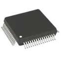
ARM® Cortex®-M4F STM32G4 Microcontroller IC 32-Bit 170MHz 512KB (512K x 8) FLASH 64-LQFP (10x10) The STM32G491RET6 from STMicroelectronics is a high-performance 32-bit microcontroller based on the Arm® Cortex®-M4 core with Floating Point Unit (FPU), designed for advanced embedded applications requiring high computational performance, precise analog processing, and real-time control. It belongs to the STM32G4 series and integrates enhanced analog peripherals, motor-control timers, communication interfaces, security features, and hardware accelerators such as CORDIC and FMAC. The device operates at up to 170 MHz, provides 512 KB Flash memory, and includes 96 KB SRAM, making it suitable for applications such as motor control, digital power conversion, industrial automation, robotics, and embedded control systems. Key Features Core: Arm® Cortex®-M4 32-bit CPU with FPU, DSP instructions, and MPU Maximum CPU Frequency: Up to 170 MHz (up to 213 DMIPS) Memory: 512 KB Flash memory with ECC support 96 KB SRAM with parity checking features Quad-SPI memory interface Operating Voltage: 1.71 V to 3.6 V Package: LQFP-64 Advanced Analog Features: 3 × 12-bit ADCs with high-speed conversion 4 × 12-bit DAC channels 4 × Rail-to-Rail operational amplifiers 4 × Fast analog comparators Internal voltage reference buffer Hardware Accelerators: CORDIC accelerator for trigonometric calculations FMAC (Filter Math Accelerator) for digital filtering applications Timers & Motor Control: Advanced PWM timers for motor-control applications Multiple 16-bit and 32-bit timers Support for encoder and PWM control Communication Interfaces: 2 × FDCAN interfaces 5 × USART/UART 3 × SPI interfaces 3 × I²C interfaces USB 2.0 Full-Speed interface SAI audio interface Security Features: True Random Number Generator (TRNG) CRC calculation unit Unique device ID Debug & Programming: SWD and JTAG debugging support Typical Applications Motor control and BLDC controllers Digital power converters Industrial automation equipment Robotics and motion control Smart sensors and embedded control systems Power management applications #STM32G491RET6 #STM32G4 #STMicroelectronics #ARM_CortexM4 #Microcontroller #MCU #EmbeddedSystems #MotorControl #DigitalPower #IndustrialAutomation #Robotics #IoT #ElectronicsDesign #PCBDesign... show more33 Uses
0 Stars
DAC80501MDGSR
16 Bit Digital to Analog Converter 1 10-VSSOP The DAC80501MDGSR is a high-precision, single-channel digital-to-analog converter developed by Texas Instruments for industrial, instrumentation, and embedded control applications requiring accurate voltage output generation. The device integrates a low-drift voltage reference, precision output buffer, and serial peripheral interface communication into a compact low-power solution optimized for high-resolution signal generation. Designed for applications such as programmable power supplies, process control systems, automated test equipment, and sensor calibration, the device delivers excellent linearity, low noise performance, and stable output characteristics across varying environmental conditions. The integrated architecture minimizes external component requirements while maintaining high accuracy and long-term reliability. The converter supports rail-to-rail output operation and offers flexible reference configurations to accommodate different system architectures. Its SPI-compatible digital interface enables straightforward integration with microcontrollers, processors, and FPGA-based systems. Electrical Characteristics The device operates from a single analog supply and supports precision voltage output generation with monotonic performance across the full operating range. Integrated precision reference circuitry provides low temperature drift and stable output characteristics suitable for high-accuracy measurement and control systems. Low glitch energy, low offset error, and low gain error characteristics improve output stability during code transitions. The output amplifier is capable of driving moderate capacitive loads while maintaining signal integrity and settling performance. Interface and Control Communication is implemented through a high-speed SPI-compatible serial interface supporting standard synchronous digital communication protocols. The interface allows direct programming of DAC output codes and internal configuration registers. The device supports daisy-chain capable serial communication architecture for simplified expansion in multi-device systems. Internal registers provide control of reference operation, power management, and output configuration functions. Power Management The DAC80501MDGSR incorporates low-power operating modes intended for energy-sensitive applications. Integrated power-down functionality reduces current consumption during inactive system states while preserving configuration integrity. Internal circuitry is optimized for low quiescent current operation without compromising output precision or dynamic response performance. Package Information The device is supplied in a compact VSSOP surface-mount package suitable for space-constrained industrial and embedded designs. The package configuration supports automated assembly processes and standard PCB manufacturing techniques. Typical Applications Typical applications include industrial automation, programmable voltage sources, data acquisition systems, sensor simulation, instrumentation equipment, motor control systems, and precision calibration platforms. The device is particularly suitable for systems requiring stable and repeatable analog voltage generation with minimal external circuitry. #commonpartslibrary #integratedcircuit #analog #digital #converter... show more30 Uses
0 Stars
7M-27.120MEEQ-T
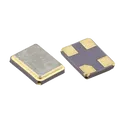
27.12 MHz ±10ppm Crystal 10pF 50 Ohms 4-SMD, No Lead # 7M-27.120MEEQ-T Crystal Unit Engineering Specification ## General Description The 7M-27.120MEEQ-T is a surface-mount quartz crystal resonator designed to provide a stable and accurate frequency reference for digital, wireless, communication, NFC, RFID, microcontroller, and embedded system applications. Manufactured by TXC Corporation, this crystal offers reliable frequency stability, low equivalent series resistance, and compact packaging suitable for space-constrained designs. Its surface-mount construction enables automated assembly while maintaining excellent electrical performance across a wide range of operating conditions. ## Features * Fundamental mode quartz crystal resonator * Surface-mount device package for automated PCB assembly * High frequency accuracy and stability * Low equivalent series resistance * Low power consumption * Suitable for clock generation and timing circuits * RoHS compliant construction * Reliable performance for industrial and consumer electronics applications ## Electrical Characteristics * Nominal Frequency: 27.120 MHz * Crystal Type: Fundamental Mode * Load Capacitance: 10 pF * Frequency Tolerance: ±20 ppm * Frequency Stability: ±20 ppm * Equivalent Series Resistance: 60 Ω Maximum * Drive Level: Low-power operation * Operating Temperature Range: Industrial grade * Storage Temperature Range: Extended environmental capability ## Mechanical Characteristics * Package Type: Surface-Mount Crystal * Mounting Style: SMD/SMT * Compact footprint optimized for high-density PCB layouts * Four-pad no-lead package construction ## Applications * PN532 NFC Controllers * RFID Readers and Writers * Microcontroller Clock Sources * Wireless Communication Modules * Embedded Systems * Industrial Control Electronics * Consumer Electronic Devices * IoT and Smart Device Platforms ## Compliance * RoHS Compliant * Lead-Free Construction * Suitable for Automated Assembly Processes #7M27_120MEEQT #TXC #CrystalResonator #SMDCrystal #QuartzCrystal #27_120MHz #PN532 #NFC #RFID #EmbeddedSystems #TimingReference #ElectronicsDesign... show more26 Uses
0 Stars
LM5010MHX/NOPB
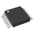
Buck Switching Regulator IC Positive Adjustable 2.5V 1 Output 1A 14-PowerTSSOP (0.173", 4.40mm Width) The LM5010 step-down switching regulator features all the functions needed to implement a low-cost, efficient, buck bias regulator capable of supplying in excess of 1-A load current. This high-voltage regulator contains an N-Channel Buck Switch, and is available in thermally enhanced 10-pin WSON and 14-pin HTSSOP packages. The hysteretic regulation scheme requires no loop compensation, resulting in fast load transient response, and simplifies circuit implementation. The operating frequency remains constant with line and load variations due to the inverse relationship between the input voltage and the ON-time. The valley current limit detection is set at 1.25 A. Additional features include: VCC undervoltage lockout, thermal shutdown, gate drive undervoltage lockout, and maximum duty cycle limiter Features 1• Input Voltage Range: 8 V to 75 V • Valley Current Limit At 1.25 A • Switching Frequency Can Exceed 1 MHz • Integrated N-Channel Buck Switch • Integrated Start-Up Regulator • No Loop Compensation Required • Ultra-Fast Transient Response • Operating Frequency Remains Constant With Load and Line Variations • Maximum Duty Cycle Limited During Start-Up • Adjustable Output Voltage • Precision 2.5-V Feedback Reference • Thermal Shutdown • Exposed Thermal Pad for Improved Heat Dissipation 2 Applications • High Efficiency Point-of-Load (POL) Regulator • Non-Isolated Telecommunications Buck Regulator • Secondary High Voltage Post Regulator • Automotive Systems #TexasInstruments #LM5010MHXNOPB #BuckRegulator #DCDCConverter #SwitchingRegulator #PowerManagement #HighVoltage #StepDownConverter #IndustrialElectronics #EmbeddedSystems #PowerSupplyDesign #HTSSOP14 #PMIC #ElectronicsDesign #VoltageRegulator... show more20 Uses
0 Stars
TLV431ACDBVT
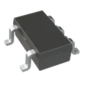
Shunt Voltage Reference IC Adjustable 1.24V 6 VV ±1% 15 mA SOT-23-5 #CommonPartsLibrary #IntegratedCircuit #PowerManagement #Voltage-reference #TLV431... show more33 Uses
0 Stars
ADS7828E/250
SOP65P640X120-16N http://www.ti.com/lit/ds/symlink/ads7828.pdf?HQS=TI-null-null-digikeymode-df-pf-null-wwe&ts=1589867963184 12-Bit, 8-Channel SAR ADC with Internal Reference and I2C Interface 1.2 Texas Instruments ADS7828E/250 595-ADS7828E/250 https://www.mouser.co.uk/ProductDetail/Texas-Instruments/ADS7828E-250?qs=%252BvKcWiXw%252BzR%252BNWlWSaV9yw%3D%3D ADS7828E/250 https://www.arrow.com/en/products/ads7828e250/texas-instruments?region=nac... show more19 Uses
0 Stars
LM4040AIZ-2.5/NOPB
Shunt Voltage Reference IC Fixed 2.5V V ±0.1% 15 mA TO-92-3 #CommonPartsLibrary #IntegratedCircuit #PowerManagement #Voltage-Reference #LM4040... show more17 Uses
0 Stars
REF5025ID
Series Voltage Reference IC Fixed 2.5V V ±0.05% 10 mA 8-SOIC #CommonPartsLibrary #IntegratedCircuit #PowerManagement #Voltage-Regulator #REF5025... show more27 Uses
0 Stars
MCP3913A1T-E/SS
MCP3913 Series 3.6 V 4.5 mA SMT Six-Channel Analog Front End - SSOP-28 The MCP3913A1T-E/SS is a high-performance, multi-channel analog front-end (AFE) from Microchip Technology intended for precision measurement applications. It features six simultaneous sampling 24-bit delta-sigma ADCs with integrated programmable gain amplifiers, enabling accurate acquisition of low-level analog signals. Designed for energy monitoring and industrial sensing, the device provides low noise, high dynamic range, and flexible configuration. It supports SPI communication for efficient interfacing with microcontrollers and digital processing systems. Key Features Six simultaneous sampling 24-bit delta-sigma ADC channels Integrated programmable gain amplifiers per channel High signal-to-noise ratio and low distortion Programmable oversampling ratios for performance tuning Internal voltage reference with external reference option SPI-compatible digital interface Configurable data output formats and control registers Low power operation modes Electrical Characteristics Resolution: 24-bit Number of Channels: 6 Input Configuration: Differential Supply Voltage: 2.7V to 3.6V Operating Temperature Range: -40°C to +125°C Programmable Gain: Up to 32 V/V (typical) Reference Voltage: Internal or external selectable Functional Description The device integrates six high-resolution delta-sigma ADCs that sample input signals simultaneously, ensuring accurate phase and timing relationships across channels. Each input passes through a programmable gain stage, allowing optimization for different sensor levels. Analog signals are digitized using oversampling and digital filtering techniques to achieve high precision and noise reduction. Configuration is handled via internal registers, and data is transferred through an SPI interface. Package Information Package Type: SSOP Pin Count: 28 Mounting Type: Surface Mount Applications Energy metering Power monitoring systems Industrial automation Multi-channel data acquisition Sensor interfacing Smart grid systems Advantages High integration reduces external components Simultaneous sampling improves measurement accuracy High resolution supports precise signal analysis Flexible configuration for various system requirements #commonpartslibrary #integratedcircuit #powermanagement #energymetering... show more14 Uses
0 Stars
DAC81416RHAT
16 Bit Digital to Analog Converter 1 40-VQFN (6x6) The DAC81416RHAT is a precision, low-power, multi-channel digital-to-analog converter designed for high-accuracy industrial and instrumentation applications. It integrates sixteen independently programmable voltage-output DAC channels with internal precision reference support, output buffering, and flexible serial communication capability. The device is optimized for systems requiring deterministic analog signal generation, high linearity, low drift, and stable long-term performance. Typical applications include automated test equipment, process control, programmable logic controllers, data acquisition systems, and closed-loop control platforms. The device supports high-resolution output generation with monotonic behavior and excellent channel-to-channel matching. Integrated diagnostic and protection features improve system reliability in harsh operating environments. The architecture is intended for dense analog output designs where low power consumption, compact footprint, and precision accuracy are critical. Engineering Specification Manufacturer: Texas Instruments Device Type: Multi-Channel Precision Voltage Output Digital-to-Analog Converter Package Type: VQFN Mounting Type: Surface Mount Channel Configuration: Sixteen independent DAC output channels DAC Resolution: High-resolution precision architecture suitable for industrial control and instrumentation systems Output Type: Buffered voltage output Interface Type: SPI-compatible serial interface Reference Support: Internal reference with external reference capability Power Supply Operation: Single-supply analog and digital operation Output Characteristics: Rail-to-rail capable buffered analog outputs with low glitch energy and fast settling behavior Linearity Performance: High integral and differential linearity with monotonic output behavior across full operating range Noise Performance: Low output noise and low temperature drift for precision signal generation Update Capability: Simultaneous and asynchronous channel update support Calibration Features: Integrated gain and offset correction support Diagnostic Features: Communication integrity monitoring and fault detection capability Industrial Features: Designed for precision automation, process control, programmable instrumentation, and multi-channel analog control systems Temperature Range: Industrial operating temperature range Protection Features: Robust serial interface handling and stable output drive architecture for industrial environments Applications: Industrial automation, programmable power control, automated test equipment, data acquisition systems, instrumentation, and closed-loop analog control platforms #commonpartslibrary #integratedcircuit #analog #digital #converter... show more12 Uses
0 Stars
dsPIC33CK256MP205-I/M4
dsPIC dsPIC™ 33CK, Functional Safety (FuSa) Microcontroller IC 16-Bit 100MHz 256KB (256K x 8) FLASH 48-UQFN (6x6) 28/36/48/64/80-Pin Digital Signal Controllers with High-Resolution PWM and CAN Flexible Data (CAN FD) Operating Conditions • 3.0V to 3.6V, -40°C to +125°C, DC to 100 MIPS • 3.0V to 3.6V, -40°C to +150°C, DC to 70 MIPS Core: 16-Bit dsPIC33CK CPU • 32-256 Kbytes of Program Flash with ECC and 8-24K RAM • Fast 6-Cycle Divide • LiveUpdate • Code Efficient (C and Assembly) Architecture • 40-Bit Wide Accumulators • Single-Cycle (MAC/MPY) with Dual Data Fetch • Single-Cycle, Mixed-Sign MUL Plus Hardware Divide • 32-Bit Multiply Support • Four Sets of Interrupt Context Saving Registers which Include Accumulator and STATUS for Fast Interrupt Handling • Zero Overhead Looping • RAM Memory Built-In Self-Test (MBIST) Clock Management • Internal Oscillator • Programmable PLLs and Oscillator Clock Sources • Reference Clock Output • Fail-Safe Clock Monitor (FSCM) • Fast Wake-up and Start-up • Backup Internal Oscillator Power Management • Low-Power Management Modes (Sleep, Idle, Doze) • Integrated Power-on Reset and Brown-out Reset High-Speed PWM • Eight PWM Pairs • Up to 250 ps PWM Resolution • Dead Time for Rising and Falling Edges • Dead-Time Compensation • Clock Chopping for High-Frequency Operation • PWM Support for: - DC/DC, AC/DC, inverters, PFC, lighting - BLDC, PMSM, ACIM, SRM motors • Fault and Current Limit Inputs • Flexible Trigger Configuration for ADC Triggering Timers/Output Compare/Input Capture • One General Purpose Timer • Peripheral Trigger Generator (PTG): - Up to 15 trigger sources to other peripheral modules - CPU independent state machine-based instruction sequencer • Nine MCCP/SCCP modules which Include Timer, Capture/Compare and PWM: - One MCCP - Eight SCCPs - 16 or 32-bit time base - 16 or 32-bit capture - 4-deep capture buffer • Fully Asynchronous Operation, Available in Sleep Modes #CommonPartsLibrary #IntegratedCircuit #Microcontroller #DSPIC33CK256MP... show more10 Uses
0 Stars
LAN8770M-I/PRA
4/4 Transceiver Full MII, RMII 32-VQFN (5x5) ## Engineering Specification ## General Description The **LAN8770M-I/PRA** is a Microchip Technology single-port **100BASE-T1 Ethernet physical layer transceiver** designed for automotive, industrial, and embedded networking applications. It provides Ethernet communication over a single balanced twisted pair and is suitable for compact systems requiring reliable network connectivity, low-power operation, and standard MAC interface support. The device is commonly used in automotive electronic control units, infotainment systems, telematics modules, sensor nodes, industrial control systems, and embedded Ethernet hardware. ## Device Identification Manufacturer Part Number: **LAN8770M-I/PRA** Manufacturer: **Microchip Technology** Product Family: **LAN8770** Device Category: **Integrated Circuit** Device Type: **Ethernet PHY Transceiver** Ethernet Standard: **100BASE-T1** Interface Type: **MII and RMII** Mounting Type: **Surface Mount** Package Type: **VQFN** ## Functional Description The device functions as an Ethernet physical layer transceiver that connects a host controller or microcontroller MAC interface to a single-pair Ethernet physical medium. It handles the analog and digital PHY functions required for 100BASE-T1 communication, allowing embedded systems to transmit and receive Ethernet data over a single twisted pair cable. ## Network and Interface Description The **LAN8770M-I/PRA** supports 100 Mb/s single-pair Ethernet communication and provides MII and RMII host interface options. This allows integration with microcontrollers, processors, gateways, and network controllers that support standard Ethernet MAC interfaces. The device is intended for applications where compact Ethernet connectivity and reduced cabling complexity are required. ## Electrical Description The device is designed for low-voltage operation and supports multiple supply domains according to the manufacturer’s recommended operating conditions. Proper power sequencing, decoupling, reset handling, clocking, and reference layout should be implemented to maintain stable PHY operation and signal integrity. ## Package and Mechanical Description The component is supplied in a compact surface-mount **VQFN package**, suitable for dense printed circuit board assemblies. The package supports automated assembly and is appropriate for space-constrained automotive and industrial electronic designs. ## Control and Diagnostic Description The PHY supports management and configuration through standard control interfaces used in Ethernet designs. It provides status monitoring and configuration capability for link management, operating mode selection, and system-level diagnostics. These features allow the host controller to configure and monitor Ethernet link behavior during operation. ## Automotive and Industrial Suitability The **LAN8770M-I/PRA** is suitable for embedded systems requiring robust single-pair Ethernet communication. It is applicable to automotive networking, telematics, infotainment, advanced driver assistance systems, industrial Ethernet nodes, building automation, control modules, and other connected embedded platforms. ## Mounting and Assembly Description The component is intended for surface-mount PCB assembly using standard reflow soldering processes. PCB layout should follow Microchip’s hardware design guidance, including proper power supply decoupling, controlled impedance routing, short signal paths, grounding, and separation of sensitive analog and digital sections where applicable. ## Design Considerations The design should account for Ethernet signal integrity, single-pair cable interface requirements, common-mode noise control, EMC performance, supply filtering, oscillator or clock source requirements, reset timing, thermal performance, and package solderability. The device should not be operated beyond the manufacturer’s specified electrical, thermal, or mechanical limits. ## Application Suitability The device is suitable for automotive Ethernet nodes, electronic control units, telematics modules, infotainment systems, sensor interfaces, industrial controllers, embedded gateways, connected equipment, and compact network-enabled hardware requiring 100BASE-T1 Ethernet PHY functionality. ## Hashtags #commonpartslibrary #integratedcircuit #ethernetphy #microchip #microchiptechnology #lan8770 #lan8770mipra #singlepairethernet #100baset1 #automotiveethernet #ethernettransceiver #phytransceiver #embeddednetworking #mii #rmii #vqfnpackage #smdcomponent #surfacemount #automotiveelectronics #industrialethernet #telematics #infotainment #embeddedhardware #pcbdesign #hardwaredesign #electronicscomponents #electronicparts #componentlibrary #engineeringparts #electronicsengineering... show more3 Uses
0 Stars
STM32F427IIT6
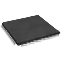
ARM® Cortex®-M4 STM32F4 Microcontroller IC 32-Bit 180MHz 2MB (2M x 8) FLASH 176-LQFP (24x24) The STM32F427IIT6 specification defines the engineering requirements for a high-performance microcontroller device designed for embedded processing applications requiring advanced computational capability, rich peripheral integration, and reliable real-time control. This specification establishes the functional, electrical, mechanical, environmental, and quality requirements necessary to ensure consistent operation across industrial, consumer, and communication systems. The device is intended for use in complex embedded systems where high-speed processing, efficient memory handling, and extensive peripheral connectivity are required. It supports applications such as industrial automation, motor control, signal processing, communication interfaces, and advanced embedded control systems. Engineering Requirements The microcontroller shall be manufactured using advanced semiconductor fabrication processes to ensure high processing performance, low power consumption, and long-term reliability. The device shall provide stable operation across its intended voltage, temperature, and environmental conditions while maintaining deterministic real-time behavior. The integrated architecture shall support high-speed processing capabilities, embedded memory resources, and multiple communication interfaces for system-level integration. Peripheral functionality shall operate reliably under defined electrical and environmental conditions without degradation of performance. Electrical characteristics shall ensure stable logic levels, accurate timing behavior, and robust signal integrity across all supported operating modes. The device shall maintain functional reliability during power transitions, reset conditions, and dynamic load variations. Mechanical and package construction shall be suitable for surface-mount assembly processes and shall ensure mechanical integrity during soldering, handling, and operation. Workmanship shall be free from defects including contamination, physical damage, or structural inconsistencies that could impact reliability or performance. Inspection, validation, and testing shall be performed using controlled procedures and calibrated equipment to ensure compliance with all applicable engineering and quality standards. Any deviation from this specification shall require formal engineering review, documented justification, and approval through the established change control process. Documentation Supporting documentation shall include engineering datasheets, reference manuals, qualification reports, electrical characterization data, inspection records, and revision-controlled manufacturing documentation. All records shall be maintained under formal configuration management and quality assurance systems. Revision Control Any modification to this specification shall be processed through the established engineering change management system. All revisions shall undergo technical review, validation, and formal approval prior to implementation to ensure continued compliance with design intent and applicable industry requirements. #EngineeringSpecification #Microcontroller #EmbeddedSystems #STMicroelectronics #DigitalControl #IndustrialElectronics #Firmware #Semiconductor #QualityAssurance #EngineeringDocumentation #RealTimeSystems... show more0 Uses
0 Stars
REF2033AIDDCT
Series Voltage Reference IC Fixed 1.65V, 3.3V V ±0.05% 20 mA SOT-23-THIN #commonpartslibrary #integratedcircuit #powermanagement #voltagereference... show more10 Uses
0 Stars
ADS1293CISQ/NOPB
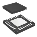
3 Channel AFE 24 Bit 28-WQFN (5x5) ADS1293CISQ/NOPB is a highly integrated, low-power 3-channel ECG Analog Front-End (AFE) from Texas Instruments. It is designed for portable and battery-powered medical devices, fitness monitors, heart-rate monitoring systems, Holter monitors, and other electrocardiogram (ECG) applications. The device integrates signal acquisition, filtering, lead-off detection, right-leg drive generation, and high-resolution analog-to-digital conversion into a single IC, reducing external component count and system cost. Key Features Three high-resolution ECG acquisition channels 24-bit analog-to-digital conversion Simultaneous pace detection support Ultra-low power consumption of approximately 0.3 mW per channel Low input-referred noise of 7 µVpp (40 Hz bandwidth) Programmable sample rates up to 25.6 ksps Differential input voltage range of ±400 mV Integrated EMI-hardened input filters Flexible input routing matrix Built-in Right-Leg Drive (RLD) amplifier AC and DC lead-off detection Integrated Wilson and Goldberger terminal generation Battery voltage monitoring capability Internal oscillator and voltage reference ALARMB pin for interrupt-driven diagnostics and fault reporting Multiple power-down and standby modes for battery-powered systems SPI-compatible digital interface Operating temperature range: –20°C to +85°C 28-pin WQFN package (5 mm × 5 mm) Typical Applications Portable 1-, 3-, 5-, 6-, 7-, 8-, and 12-lead ECG systems Holter monitors Event recorders Telemedicine devices Patient vital-sign monitoring equipment Automated External Defibrillators (AEDs) Sports and fitness heart-rate monitors Wearable medical devices Hashtags #commonpartslibrary #integratedcircuit #TexasInstruments #ADS1293 #AFE #AnalogFrontEnd #ECG #Electrocardiogram #MedicalElectronics #HealthTech #WearableDevices #HeartRateMonitor #PatientMonitoring #BiomedicalEngineering #24BitADC #LowPowerDesign #SPI #SignalConditioning #PortableMedicalDevices #HolterMonitor #Telemedicine #VitalSignsMonitoring #EmbeddedSystems #MixedSignalIC #WQFN28 #BatteryPoweredDevices #MedicalInstrumentation... show more3 Uses
0 Stars
ADPD7000BCBZR7
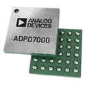
4 Channel AFE 12 Bit 36-WLCSP (2.8x2.56) The ADPD7000 is a highly integrated analog front end (AFE) designed for measuring various vital signals. The optical channel is designed as an optical transceiver, stimulating up to eight light emitting diodes (LEDs) and measuring the return signal on up to four separate current inputs. The signal chain rejects signal offsets and corruption from asynchronous modulated interference, typically from ambient light, eliminating the need for optical filters or externally controlled DC cancellation circuitry. The electrocardiography (ECG) signal acquisition is designed to support low noise, diagnostic level measurement in the presence of a variety of interferers. The ECG signal chain has a number of complementary features supporting ECG measurement, such as driven reference for common-mode rejection and lead off detection to identify a fallen electrode. The body impedance analysis (BIA) signal chain is designed for body impedance measurement with a configurable excitation path and measurement path. A 12-bit digital-to-analog converter (DAC) is used in the excitation path to generate the sinusoid wave and high precision measurement, with configurable filters used to measure the body response of the stimulus. The electrodermal activity (EDA) signal chain is designed for electrodermal activity. By multiplexing BIA and ECG peripheral circuits, the ADPD7000 supports high precision AC and DC measurement with 1 nS resolution. The data output and functional configuration use a serial port interface (SPI) on the ADPD7000. The control circuitry includes flexible LED signaling and synchronous detection, digital filters, digital wave generators, and configurable filters. The ADPD7000 is available in a 2.795 mm × 2.560 mm, 0.40 mm pitch, 36-ball WLCSP. ► Multimodal analog front end ► Optical channel ► 4 input channels with multiple operation modes for various sensor measurements ► 4-channel processing with simultaneous sampling ► 12 programmable time slots for synchronized sensor measurements ► Flexible input multiplexing to support single-ended sensor measurements ► 8 LED drivers, 2 of which can be driven simultaneously ► Flexible sampling rate from 0.004 Hz to 9 kHz using internal oscillators ► AC ambient light rejection: 78 dB up to 100 Hz ► 400 mA total LED peak drive current ► Individual ambient cancellation DAC at TIA input with 9-bit control up to 300 μA ► Individual LED DC cancellation DAC at TIA input with 7-bit control up to 190 μA ► ECG channel ► <1 µV RMS RTI noise at diagnosis bandwidth ► High input impedance 20 GΩ ► Accepts up to ±1.2 V of DC differential input range ► CMRR: 115 dB ► Flexible 4 electrode configurations to support various applications ► Both AC lead off detection and DC lead off detection ► Support always on, low power, lead on detection ► BIA channel ► Low power, high accuracy excitation path ► Configurable excitation frequency up to 250 kHz ► Sine wave excitation with a 12-bit DAC ► High accuracy with large imbalance contact impedance ≤20 kΩ ► Configurable receive filters with low noise design ► Complex impedance measurement engine ► Integrated current-limit resistors ► EDA channel ► Support both voltage excitation and current excitation ► 10 kΩ to100 MΩ measurement range with 1 nS resolution ► DFT and decimation for high accuracy measurement result ► SPI communications supported ► 704-byte FIFO... show more9 Uses
0 Stars
REF3025AIDBZT
Series Voltage Reference IC Fixed 2.5V V ±0.2% 25 mA SOT-23-3 #ReferenceVoltaget #commonpartslibrary... show more22 Uses
0 Stars
ADS1263IPW
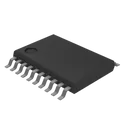
32 Bit Analog to Digital Converter 5, 10 Input 1 Sigma-Delta 28-TSSOP The ADS1263IPW is a high-precision, low-noise analog-to-digital converter designed for demanding industrial, instrumentation, and sensor measurement applications. Manufactured by Texas Instruments, this device integrates a delta-sigma ADC architecture with programmable gain amplification, precision voltage reference support, sensor biasing functions, and extensive diagnostic capabilities. It is optimized for applications requiring extremely high resolution and accuracy when measuring low-level analog signals. The device supports direct interfacing to bridge sensors, thermocouples, RTDs, pressure sensors, strain gauges, and other precision transducers. Integrated system monitoring and fault detection features simplify implementation in safety-critical and high-reliability systems. Flexible input multiplexing and multiple data-rate options allow the converter to be used across a wide range of precision data acquisition applications. The ADS1263IPW communicates through a standard SPI-compatible serial interface and operates from low-voltage analog and digital supplies. The device is packaged in a thermally efficient TSSOP package suitable for compact embedded system designs. Electrical Characteristics The converter utilizes a delta-sigma ADC core with extremely high effective resolution and low input-referred noise performance. It supports differential and single-ended analog input configurations with programmable gain settings for low-level sensor measurements. The integrated programmable gain amplifier supports multiple gain selections for direct amplification of small analog signals. The converter includes internal offset and gain calibration functions to improve system-level measurement accuracy. The device provides low drift characteristics and high common-mode rejection performance suitable for precision industrial environments. Analog Features The converter supports multiple analog input channels through an integrated input multiplexer. Internal sensor bias current sources are available for RTD and resistive sensor excitation applications. Integrated digital filtering options allow optimization between noise performance and conversion speed. Simultaneous rejection of power-line interference frequencies is supported for industrial measurement systems. The device includes internal temperature sensing and diagnostic monitoring functions for enhanced system reliability. Digital Interface Communication is implemented through an SPI-compatible serial interface supporting flexible host controller integration. The interface supports command-based register access, data readback, and configuration management. Programmable data rates allow balancing between throughput and precision requirements. Power Requirements The device operates from separate analog and digital supply rails to improve noise isolation and measurement accuracy. Low-power operating modes are supported for energy-sensitive applications. Protection and Diagnostics Integrated fault detection and monitoring functions include sensor open-circuit detection, reference monitoring, supply monitoring, and internal self-test capability. These features improve reliability in industrial and safety-oriented systems. Package Information The ADS1263IPW is supplied in a TSSOP package with fine-pitch lead spacing suitable for high-density PCB layouts and automated assembly processes. Typical Applications Industrial process control systems Precision data acquisition equipment Temperature measurement systems Pressure and bridge sensor interfaces Weigh scale and load-cell instrumentation Laboratory and test instrumentation Medical instrumentation Energy monitoring and metering systems #commonpartslibrary #integratedcircuit #analog #digital #converter... show more6 Uses
0 Stars
PCM5102AQPWRQ1
Audio D/A Converter ICs 2VRMS DirectPath Aud io Stereo DAC 20-TSSOP The PCM5102AQPWRQ1 specification defines the engineering requirements for an automotive-grade digital-to-analog audio converter integrated circuit intended for high-performance digital audio applications. The specification establishes the functional, electrical, mechanical, thermal, and quality requirements necessary to ensure reliable conversion of digital audio signals into high-fidelity analog outputs. It serves as the governing technical reference for component selection, system integration, manufacturing, verification, and quality assurance throughout the product lifecycle. The device is designed to provide high-resolution audio performance with low distortion, low noise, and stable operation under automotive environmental conditions. It is suitable for use in infotainment systems, digital audio processing equipment, communication systems, and other embedded electronic applications requiring reliable digital-to-analog signal conversion. Engineering Requirements The component shall be manufactured using qualified semiconductor fabrication processes and approved materials to ensure consistent electrical performance, mechanical integrity, and long-term reliability. The device shall comply with applicable automotive qualification requirements and maintain stable operation within its specified voltage, temperature, and environmental operating ranges. Electrical performance shall meet the specified requirements for signal integrity, dynamic range, total harmonic distortion, noise performance, and output accuracy. The package shall be compatible with standard surface-mount assembly processes and shall withstand soldering and handling conditions without degradation. Workmanship shall be free from physical defects, contamination, package damage, or manufacturing irregularities that could affect functionality or reliability. Inspection, testing, and validation shall be performed using calibrated equipment and controlled procedures to verify compliance with all applicable engineering and quality requirements. Any deviation from this specification shall require formal engineering evaluation, documented technical justification, and approved change authorization prior to implementation. Documentation Supporting documentation shall include engineering drawings, electrical specifications, qualification reports, material declarations, inspection records, manufacturing documentation, and revision-controlled technical files. All documentation shall be maintained in accordance with established engineering configuration management and quality control procedures. Revision Control Changes to this specification shall be managed through the formal engineering change control process. All revisions shall undergo technical review, validation, and approval to ensure continued compliance with design intent, automotive quality standards, and applicable regulatory requirements. #EngineeringSpecification #AutomotiveElectronics #DigitalToAnalogConverter #AudioEngineering #EmbeddedSystems #QualityAssurance #Semiconductor #EngineeringDocumentation #Compliance #CommonPartsLibrary #IntegratedCircuit #Data-Acquisition #ADCs #DACs #PCM5102... show more4 Uses
0 Stars
LM336Z-2.5/LFT3
Shunt Voltage Reference IC Fixed 2.49V V ±4% 10 mA TO-92-3 #ReferenceVoltage #commonpartslibrary #IntegratedCircuit #Power-Management #LM336... show more7 Uses
0 Stars
LM4040C25IDBZR
Shunt Voltage Reference IC Fixed 2.5V V ±0.5% 15 mA SOT-23-3 #commonpartslibrary #integratedcircuit #powermanagement #voltagereference... show more7 Uses
0 Stars