TPS7A2030PDBVR
Low-Noise Low-Dropout (LDO) Voltage Regulator – Fixed 3.0 V positive-output LDO regulator providing up to 300 mA output current for low-noise power regulation. Operates from a 1.6 V to 6.0 V input voltage, features 140 mV maximum dropout voltage at 300 mA, 15 µA typical quiescent current, 65 dB to 40 dB PSRR (100 Hz to 1 MHz), and an enable input for power management. Includes overcurrent protection, thermal shutdown, and undervoltage lockout (UVLO). Specified for an operating junction temperature range of −40°C to +125°C and housed in a 5-pin SOT-23 (DBV) package. #TexasInstruments #TPS7A2030PDBVR #LDO #VoltageRegulator #LowDropout #300mA #3V #LowNoise #PowerManagement #SOT23 #EmbeddedSystems #PMIC... show more2 Uses
0 Stars

TPD2EUSB30
2-Channel ESD Protection for Super-Speed USB 3.0 Interface, DRT-3 ESD protection USB 3.0 Texas*DRT*... show more167 Uses
1 Star
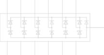
TPD6E05U06RVZ
6-Channel ESD Protection for Super-Speed USB 3.0 Interface, USON-14 ESD protection USB 3.0 Texas*PUSON*14*... show more163 Uses
0 Stars
LM66100-Q1
Automotive 1.5-V to 5.5-V, 1.5-A, 0.5-µA IQ ideal diode with integrated FET The LM66100-Q1 is a Single-Input, Single-Output (SISO) integrated ideal diode that is well suited for a variety of applications. The device contains a Pchannel MOSFET that can operate over an input voltage range of 1.5 V to 5.5 V and can support a maximum continuous current of 1.5 A. The chip enable works by comparing the CE pin voltage to the input voltage. When the CE pin voltage is higher than VIN, the device disables and the MOSFET is off. When the CE pin voltage is lower, the MOSFET is on. The LM66100-Q1 also comes with reverse polarity protection (RPP) that can protect the device from a miswired input, such as a reversed battery. Two LM66100-Q1 devices can be used in an ORing configuration similar to a dual diode ORing implementation. In this configuration, the devices pass the highest input voltage to the output while blocking reverse current flow into the input supplies. These devices can compare input and output voltages to make sure that reverse current is blocked through an internal voltage comparator. The LM66100-Q1 is available in a standard SC-70 package characterized for operation over a junction temperature range of –40°C to 150°C. 1 Features • AEC-Q100 qualified for automotive applications: – Device temperature grade 1: –40°C to 125°C ambient operating temperature range • Wide operating voltage range: 1.5 V–5.5 V • Reverse voltage standoff on VIN: –6-V absolute maximum • Maximum continuous current (IMAX): 1.5 A • On-Resistance (RON): – 5-V VIN = 79 mΩ (typical) – 3.6-V VIN = 91 mΩ (typical) – 1.8-V VIN = 141 mΩ (typical) • Comparator chip enable (CE) • Channel status indication (ST) • Low current consumption: – 3.6-V VIN shutdown current (ISD,VIN): 120 nA (typical) – 3.6-V VIN quiescent current (IQ, VIN): 150 nA (typical)... show more58 Uses
0 Stars

