Boost Converter Project Overview
1:38
General (prev)
Project
Below is an overview of the project based on its current design context:
Purpose and Concept
-
Objective:
The project is a breakout board centered on the MT3608 DC‐DC step‐up converter. It is intended to deliver a boosted voltage (up to 28 V) from a lower LiPo battery voltage for an Arduino shield designed to charge LiPo cells. Essentially, it acts as the power conversion engine for the charger, ensuring that the input voltage is stepped up to the level needed by the rest of the circuit. -
Design Intent:
The board is designed for a compact layout (for example, it features a SOT-23-6 package for the main converter) with careful routing of power nets and ground, along with the placement of essential passive components to support high-frequency operation. The design embodies a “breakout” strategy that provides connection points for external circuits via terminals for VIN+, VIN–, VOUT+, and VOUT–.
Core Components and Their Roles
-
MT3608 Boost Converter (MT3608)
- Role: The heart of the circuit, the MT3608 is a high-efficiency boost converter. It regulates the boosted output voltage using internal feedback and an external resistor divider network.
- Key Pins and Functions:
- IN/EN: Accepts the input voltage and controls the conversion mode (enable function).
- FB: Receives feedback from an external resistor network to regulate the output voltage.
- SW and GND: Work together with the inductor to complete the boost switching cycle.
-
Passive Components
- Input and Output Capacitors (C3 and C4):
- Provide decoupling for noise reduction and voltage stability on both the input and the output.
- Resistors (R1, R3, R4):
- Form the voltage divider for the feedback pin on MT3608.
- Serve other functions such as current sensing or potential pull-up/pull-down purposes.
- Inductor (SMRH74-220MT designated as U2):
- Works in tandem with the switch (SW) of the MT3608 for energy storage during the switching cycle.
- Input and Output Capacitors (C3 and C4):
-
Diode (SS34)
- Role: Provides rectification and prevents reverse current flow. In a boost converter, this diode is critical for ensuring that the inductor’s stored energy transfers to the output capacitor during the off-cycle of the switching transistor.
-
Interconnection Elements (Net Portals / Terminals)
- The project includes dedicated nets for VIN+, VIN–, VOUT+, and VOUT– that serve as connection points. These “Net Portal” and terminal symbols allow the designer to interface external wiring with the board.
Design and Implementation Breakdown
-
Schematic Level
- The converter (MT3608) is placed in the schematic with its associated passive support network (feedback resistors, decoupling capacitors, inductor, and diode).
- Nets are defined to connect the input, output, ground, and feedback pins. For example, the net “U1 – IN” connects the input voltage through the terminal and capacitor filters.
- Control and enable signals are tied directly to the converter so that the unit can be switched on or off as needed.
-
PCB Layout Considerations
- The board is designed with a compact two-layer stack-up. Critical considerations include minimizing the length of high-current traces (especially those carrying the switching currents through the inductor and diode) and maintaining a solid ground plane.
- PCB rules and design overrides are in place for critical objects such as via placements (to ensure proper grounding) and text labels (keeping designators clear in 3D view).
- The layout shows careful placement of components to reduce parasitic inductance and resistance, which is especially important for high-frequency boost converters.
-
Manufacturing and Assembly
- The design includes well-defined footprints for all SMD components (for example, the SOT-23-6 package for the MT3608 and SMD footprints for capacitors and resistors).
- The review reports indicate that there are areas with overlapping copper and component override issues. While these do not prevent manufacturing, they may need to be addressed to avoid potential shorts or misrouted connections.
- DRC and review checks (such as for airwires and missing footprints) are part of the design verification process before manufacturing.
Design Choices, Trade-offs, and Key Technologies
-
Chosen Converter (MT3608):
Using the MT3608 allows for a compact, high-frequency boost converter solution. Its SOT-23-6 package minimizes board area but may challenge thermal performance at higher currents. -
Feedback Network:
The use of passive resistors for voltage sensing involves a trade-off between accuracy and board real estate. The resistor values are selected per the datasheet recommendations, with additional decoupling to filter high-frequency noise. -
Component Footprints and Placement:
The decision to use industry-standard SMD footprints (such as for 0603 passive components) helps in rapid prototyping; however, it necessitates careful placement due to tight spacing which can complicate routing. -
PCB Layout Constraints:
A two-layer board requires extra attention to routing high-current paths and keeping the ground network robust. This is a trade-off between cost and performance compared to a multilayer board.
Potential Challenges and Performance Considerations
-
Thermal Management:
Due to the small package sizes and high switching frequencies, ensuring that the MT3608 and the inductor maintain acceptable temperatures under load is critical. -
Circuit Efficiency:
Losses in the diode and inductor as well as in the switching network can affect efficiency. Optimizing the routing (minimizing trace lengths and using proper via sizes) is important. -
EMI/EMC Concerns:
Boost converters are sources of electrical noise. Adequate decoupling and layout separation between high-frequency switching nodes and sensitive analog sections are necessary. -
Review Errors and DRC Violations:
The review summary indicates issues such as overlapping copper and airwires that have not been resolved. Addressing these is important before sending the design for manufacturing.
Real-World Applications and Future Enhancements
-
Applications:
This design can serve as a building block in portable LiPo charging systems for Arduino-based projects. It is applicable in battery-powered systems where a regulated boost converter is needed to achieve a higher, stable voltage. -
Areas for Improvement:
- Layout Refinement: Addressing the review errors (for instance, optimizing trace widths, via placements, and copper fills) could help increase reliability.
- Thermal Optimization: Consider adding thermal vias or copper pours to better manage heat dissipation.
- Component Optimization: Evaluate alternative components or more integrated solutions if board space and efficiency become critical.
- Scalability: For higher current applications, upgrading to a converter with integrated power switches or using a multilayer PCB for additional power and ground planes might be considered.
- EMI Filtering: Additional filtering can be implemented if interference with sensitive parts is identified during real-world testing.
In summary, the project is a dedicated MT3608-based boost converter breakout board for a LiPo charger Arduino shield. Its design carefully integrates the main converter, the supporting passive network, and interconnect terminals within the constraints of a compact two-layer PCB. Addressing minor review and layout issues while keeping an eye on thermal and electromagnetic performance will be key to ensuring robust operation in real-world applications.
Review and resolve DRC errors
Improve thermal management
Consider EMI mitigation strategies
356 days
Ready.
U1
VIN+
D2
C4
Capacitance
22u F
R1
Resistance
1.8k Ω
R3
Resistance
1k
Ω
U2
Inductance
22u H
Reviews
Electrical Rule Checks
Duplicate Designators
Reports components with identical designators.
No-Connect Violation
Reports no-connect pins that are connected.
Pin-to-Pin Conflicts
Reports incompatible pin connections on the same net based on electrical pin types.
Shorted Components
Reports any 2-pin component with both pins connected to the same net.
Missing Power
Reports power input pins that are not connected to a power source.
Single Pin Nets
Reports nets that have only one pin connected.
Missing Designator
Reports components without a designator.
Design Rule Checks
Overlapping Copper • 1
Des | Net | Des | Net | ... | |
|---|---|---|---|---|---|
None |
Reports copper elements that are shorting.
Invalid Layer
Reports nodes that are assigned to a layer that doesn't exist in the layout stackup.
Component Overrides • 9
Reports components that have been modified using the "!important" flag.
Airwires • 6
Reports missing routed traces between pads in a net.
Layers with Multiple Fills
Reports layers that have multiple copper fills of different nets. Make sure the Connected Layers rule value of nets with fills is valid.
Floating Copper • 3
Detect any via, trace or copper fill island that is not connected to any net.
Protected Intrusions
Reports intrusions from objects of other nets into polygons or fills that have the Protected layout rule applied.
Missing Footprints
Reports components that need a footprint but don't have one.
Manufacturing
Manufacturer Part Number
Reports components that have no manufacturer part number.
Parts Available
BetaChecks that all components are available from distributors.
Component Review Checks
Incomplete Project Info
Reports the project when the name or description haven't been modified from the default.
Missing Properties
Reports the project or terminals when critical properties are missing: Manufacturer Part Number, Manufacturer Name, Datasheet, Part Type, Designator Prefix, or Pin Number.
Missing Terminals
Reports the project when no terminals are present.
Missing Parametric Symbol Properties
Reports terminals that are missing parametric symbol properties (pin group, pin orientation, section).
System Checks
Auto-Layout
BetaReports issues with Auto-Layout if Flux cannot route something or must ignore a configuration.
Passive Components
Resistor Power Rating
BetaChecks that the power traveling across a given resistor is under its rating with 50% headroom.
Learn morePull Up/Pull Down Presence
BetaChecks that IC pins that require pull up or pull down resistors have them.
Learn moreCapacitor Voltage Rating
BetaChecks that capacitors have appropriate voltage ratings to prevent overheating and ensure reliable circuit operation.

- Wirelessly connects nets on schematic. Used to organize schematics and separate functional blocks. To wirelessly connect net portals, give them same designator. #portaljharwinbarrozo43.0M
- Wirelessly connects power nets on schematic. Identical to the net portal, but with a power symbol. Used to organize schematics and separate functional blocks. To wirelessly connect power net portals, give them the same designator. #portal #powerjharwinbarrozo11.4M
- A generic fixed resistor for rapid developing circuit topology. Save precious design time by seamlessly add more information to this part (value, footprint, etc.) as it becomes available. Standard resistor values: 1.0Ω 10Ω 100Ω 1.0kΩ 10kΩ 100kΩ 1.0MΩ 1.1Ω 11Ω 110Ω 1.1kΩ 11kΩ 110kΩ 1.1MΩ 1.2Ω 12Ω 120Ω 1.2kΩ 12kΩ 120kΩ 1.2MΩ 1.3Ω 13Ω 130Ω 1.3kΩ 13kΩ 130kΩ 1.3MΩ 1.5Ω 15Ω 150Ω 1.5kΩ 15kΩ 150kΩ 1.5MΩ 1.6Ω 16Ω 160Ω 1.6kΩ 16kΩ 160kΩ 1.6MΩ 1.8Ω 18Ω 180Ω 1.8KΩ 18kΩ 180kΩ 1.8MΩ 2.0Ω 20Ω 200Ω 2.0kΩ 20kΩ 200kΩ 2.0MΩ 2.2Ω 22Ω 220Ω 2.2kΩ 22kΩ 220kΩ 2.2MΩ 2.4Ω 24Ω 240Ω 2.4kΩ 24kΩ 240kΩ 2.4MΩ 2.7Ω 27Ω 270Ω 2.7kΩ 27kΩ 270kΩ 2.7MΩ 3.0Ω 30Ω 300Ω 3.0KΩ 30KΩ 300KΩ 3.0MΩ 3.3Ω 33Ω 330Ω 3.3kΩ 33kΩ 330kΩ 3.3MΩ 3.6Ω 36Ω 360Ω 3.6kΩ 36kΩ 360kΩ 3.6MΩ 3.9Ω 39Ω 390Ω 3.9kΩ 39kΩ 390kΩ 3.9MΩ 4.3Ω 43Ω 430Ω 4.3kΩ 43KΩ 430KΩ 4.3MΩ 4.7Ω 47Ω 470Ω 4.7kΩ 47kΩ 470kΩ 4.7MΩ 5.1Ω 51Ω 510Ω 5.1kΩ 51kΩ 510kΩ 5.1MΩ 5.6Ω 56Ω 560Ω 5.6kΩ 56kΩ 560kΩ 5.6MΩ 6.2Ω 62Ω 620Ω 6.2kΩ 62KΩ 620KΩ 6.2MΩ 6.8Ω 68Ω 680Ω 6.8kΩ 68kΩ 680kΩ 6.8MΩ 7.5Ω 75Ω 750Ω 7.5kΩ 75kΩ 750kΩ 7.5MΩ 8.2Ω 82Ω 820Ω 8.2kΩ 82kΩ 820kΩ 8.2MΩ 9.1Ω 91Ω 910Ω 9.1kΩ 91kΩ 910kΩ 9.1MΩ #generics #CommonPartsLibraryjharwinbarrozo1.5M
- A generic fixed capacitor ideal for rapid circuit topology development. You can choose between polarized and non-polarized types, its symbol and the footprint will automatically adapt based on your selection. Supported options include standard SMD sizes for ceramic capacitors (e.g., 0402, 0603, 0805), SMD sizes for aluminum electrolytic capacitors, and through-hole footprints for polarized capacitors. Save precious design time by seamlessly add more information to this part (value, footprint, etc.) as it becomes available. Standard capacitor values: 1.0pF 10pF 100pF 1000pF 0.01uF 0.1uF 1.0uF 10uF 100uF 1000uF 10,000uF 1.1pF 11pF 110pF 1100pF 1.2pF 12pF 120pF 1200pF 1.3pF 13pF 130pF 1300pF 1.5pF 15pF 150pF 1500pF 0.015uF 0.15uF 1.5uF 15uF 150uF 1500uF 1.6pF 16pF 160pF 1600pF 1.8pF 18pF 180pF 1800pF 2.0pF 20pF 200pF 2000pF 2.2pF 22pF 20pF 2200pF 0.022uF 0.22uF 2.2uF 22uF 220uF 2200uF 2.4pF 24pF 240pF 2400pF 2.7pF 27pF 270pF 2700pF 3.0pF 30pF 300pF 3000pF 3.3pF 33pF 330pF 3300pF 0.033uF 0.33uF 3.3uF 33uF 330uF 3300uF 3.6pF 36pF 360pF 3600pF 3.9pF 39pF 390pF 3900pF 4.3pF 43pF 430pF 4300pF 4.7pF 47pF 470pF 4700pF 0.047uF 0.47uF 4.7uF 47uF 470uF 4700uF 5.1pF 51pF 510pF 5100pF 5.6pF 56pF 560pF 5600pF 6.2pF 62pF 620pF 6200pF 6.8pF 68pF 680pF 6800pF 0.068uF 0.68uF 6.8uF 68uF 680uF 6800uF 7.5pF 75pF 750pF 7500pF 8.2pF 82pF 820pF 8200pF 9.1pF 91pF 910pF 9100pF #generics #CommonPartsLibraryjharwinbarrozo1.5M
- A generic fixed inductor for rapid developing circuit topology. *You can now change the footprint and 3D model at the top level anytime you want. This is the power of #genericsjharwinbarrozo15.4k
- An electrical connector acting as reusable interface to a conductor and creating a point where external circuits can be connected.Terminal
- 47 kOhms ±5% 0.125W, 1/8W Chip Resistor 0805 (2012 Metric) Automotive AEC-Q200 Thick Film #forLedBlinkjharwinbarrozo1.2M
- 10uF Capacitor Aluminum Polymer 20% 16V SMD 5x5.3mm #forLedBlink #commonpartslibrary #capacitor #aluminumpolymer #radialcanjharwinbarrozo1.2M
- Yellow 595nm LED Indication - Discrete 1.7V 1206 (3216 Metric) #forLedBlinkjharwinbarrozo1.1M


Inspect
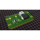
MT3608 Breakout Board Rev C x5KH
Controls
Properties
Designator Prefix
sublayout
Availability & Pricing
| Distributor | Qty 1 | |
|---|---|---|
| Arrow | $0.18–$0.64 | |
| Digi-Key | $0.10–$1.25 | |
| LCSC | $0.29–$0.68 | |
| Mouser | $1.00–$1.21 | |
| Verical | $0.07–$0.48 | |
Assets
 3600_3_09.svg
id=3600_3_09
 revcqr.svg
id=revcqr
- 3296W-1-104LF.STEP
id=3296W-1-104LF
- thumbnail.PNG
id=thumbnail
Default
3d Model
Thumbnail

Welcome 👋
Flux helps you build PCBs faster with an AI teammate!
Create your account to collaborate, stay updated, fork your own version, and get instant answers from our AI agent.