
DS1307+
64 x 8, Serial, I2C Real-time clock, 4.5V to 5.5V VCC, 0°C to +70°C, DIP-8 RTC, Trickle-Charge Timekeeping Chip DIP*W7.62mm*... show more10 Uses
0 Stars

DS1302Z+
Trickle-Charge Timekeeping Chip, 2.0V to 5.5V VCC, 0°C to +70°C, SOIC-8 RTC, Trickle-Charge Timekeeping Chip SOIC*3.9x4.9mm?P1.27mm*... show more1 Use
0 Stars
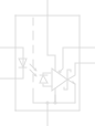
HCPL-2601
Single High Speed LSTTL/TTL Compatible Optocoupler with enable, dV/dt 10000V/us, VCM 1000, max 7V VCC, DIP-8 High speed optically coupled gates enable DIP*W7.62mm*... show more0 Uses
0 Stars
BP2866C
The BP2866C, manufactured by 晶丰明源半导体, is a high precision buck constant current LED driver designed for universal input offline LED lighting applications. Operating in critical conduction mode, this component is suitable for 85Vac~265Vac input and integrates a 500V power MOSFET. It features patented demagnetization detection technology and high-voltage JFET power supply technology, eliminating the need for a VCC capacitor and starting resistors, thereby minimizing system cost and size. The BP2866C offers precise output current and excellent line regulation through a patent-pending current control method. It includes robust protection functions such as LED short circuit protection, VCC under voltage protection, and thermal regulation. Available in a SOP7 package, it ensures a +5% LED output current accuracy and is ideal for applications like LED candle lights and bulbs.... show more1 Use
0 Stars
LM5010MHX/NOPB
Buck Switching Regulator IC Positive Adjustable 2.5V 1 Output 1A 14-PowerTSSOP (0.173", 4.40mm Width) The LM5010 step-down switching regulator features all the functions needed to implement a low-cost, efficient, buck bias regulator capable of supplying in excess of 1-A load current. This high-voltage regulator contains an N-Channel Buck Switch, and is available in thermally enhanced 10-pin WSON and 14-pin HTSSOP packages. The hysteretic regulation scheme requires no loop compensation, resulting in fast load transient response, and simplifies circuit implementation. The operating frequency remains constant with line and load variations due to the inverse relationship between the input voltage and the ON-time. The valley current limit detection is set at 1.25 A. Additional features include: VCC undervoltage lockout, thermal shutdown, gate drive undervoltage lockout, and maximum duty cycle limiter Features 1• Input Voltage Range: 8 V to 75 V • Valley Current Limit At 1.25 A • Switching Frequency Can Exceed 1 MHz • Integrated N-Channel Buck Switch • Integrated Start-Up Regulator • No Loop Compensation Required • Ultra-Fast Transient Response • Operating Frequency Remains Constant With Load and Line Variations • Maximum Duty Cycle Limited During Start-Up • Adjustable Output Voltage • Precision 2.5-V Feedback Reference • Thermal Shutdown • Exposed Thermal Pad for Improved Heat Dissipation 2 Applications • High Efficiency Point-of-Load (POL) Regulator • Non-Isolated Telecommunications Buck Regulator • Secondary High Voltage Post Regulator • Automotive Systems #TexasInstruments #LM5010MHXNOPB #BuckRegulator #DCDCConverter #SwitchingRegulator #PowerManagement #HighVoltage #StepDownConverter #IndustrialElectronics #EmbeddedSystems #PowerSupplyDesign #HTSSOP14 #PMIC #ElectronicsDesign #VoltageRegulator... show more19 Uses
0 Stars
M24256E-FMN6TP
EEPROM Memory IC 256Kbit I2C 1 MHz 450 ns 8-SO The M24256E-FMN6TP is a 256-Kbit (32 Kbyte) I²C-compatible serial EEPROM from STMicroelectronics. It is designed for reliable, non-volatile data storage in a wide range of electronic applications including consumer, industrial, and automotive systems. The device supports standard (100 kHz), fast (400 kHz), and fast-mode plus (1 MHz) I²C communication, enabling efficient data transfer. It features byte and page write operations, low power consumption, and a high endurance of write cycles, making it suitable for frequent data logging and configuration storage. Housed in a compact SO8 package, the device is optimized for space-constrained PCB designs while maintaining robust performance and data retention capabilities. Key Features Memory size: 256 Kbit (32 Kbyte) Interface: I²C (2-wire serial interface) Clock frequency: Standard mode: 100 kHz Fast mode: 400 kHz Fast-mode Plus: 1 MHz Supply voltage range: 1.7 V to 5.5 V Page write capability: up to 64 bytes Write cycle time: ~5 ms (typical) Data retention: > 200 years Endurance: > 4 million write cycles Hardware write protection available ESD protection and latch-up immunity Functional Description The device operates as a slave on the I²C bus and supports: Byte write and read Page write (up to 64 bytes) Random and sequential read operations Memory addressing is internally managed using a 16-bit address pointer, allowing access to the full 32 KB memory array. The device includes an internal write cycle controller, eliminating the need for external timing management. Pin Configuration (SO8 Package) A0, A1, A2: Device address inputs VSS: Ground SDA: Serial data line SCL: Serial clock line WC: Write control (hardware write protection) VCC: Supply voltage Absolute Maximum Ratings Supply voltage (VCC): -0.3 V to 6.5 V Input voltage: -0.3 V to VCC + 0.6 V Storage temperature: -65°C to +150°C Operating temperature (industrial grade): -40°C to +85°C Electrical Characteristics Low standby current: < 1 µA (typical) Operating current: < 1 mA Input/output compatible with CMOS logic levels Schmitt trigger inputs for noise immunity Timing Characteristics Write cycle time: 5 ms (typical) Fast-mode Plus support up to 1 MHz Sequential read supports continuous data streaming Package Information Package type: SO8 (8-lead Small Outline) Mounting: Surface-mount (SMD) Tape & reel packaging (TP suffix) Applications Configuration storage Calibration data storage Data logging systems Industrial control systems Consumer electronics Embedded systems requiring non-volatile memory Advantages High endurance and long data retention Wide voltage range (ideal for mixed-voltage systems) Compact footprint High-speed I²C compatibility (up to 1 MHz) #commonpartslibrary #integratedcircuit #memory... show more14 Uses
0 Stars
VNI2140J
Power Switch/Driver 1:1 N-Channel 500mA PowerSSO-12 8-channel protected high-side 12 V output switch IC The VNI2140J is a monolithic device designed using STMicroelectronics' VIPower technology. The device drives two independent resistive or inductive loads with one side connected to ground. Active current limitation prevents a drop in system power supply in cases of shorted-load, and built-in thermal shutdown protects the chip from damage due to overtemperature and short-circuit. In overload conditions, channel turns OFF and ON automatically to maintain the junction temperature between TTSD and TR. If the case temperature reaches TCSD, the overloaded channel is turned OFF and restarts only when case temperature decreases down to TCR. In order to avoid high-peak current from the supply, when more than one channel is overloaded the TCSD restart is not simultaneous. Non overloaded channels continue to operate normally. The open-drain diagnostics output indicates overtemperature conditions and open-load in OFF-state. Features • Nominal current: 0.75 A per channel • Shorted-load protections • Junction overtemperature protection • Case overtemperature protection for thermal independence of the channels • Thermal case shutdown restart not simultaneous for the various channels • Protection against loss of ground • Current limitation 1 A per channel • Undervoltage shutdown • Open-load in OFF-state and short to VCC detection • Open-drain diagnostic outputs • 3.3 V CMOS/TTL compatible inputs • Fast demagnetization of inductive loads • Conforms to IEC 61131-2 Applications • Programmable logic control • Industrial PC peripheral input/output • Numerical control machines #VNI2140J #STMicroelectronics #VIPower #HighSideSwitch #SolidStateRelay #PowerManagement #IndustrialAutomation #PLC #LoadDriver #PowerSSO12... show more7 Uses
0 Stars
ADXL335BCPZ-RL7
Accelerometer X, Y, Z Axis ±3g 1.6kHz (X,Y), 550Hz (Z) 16-LFCSP-LQ (4x4) The ADXL335BCPZ-RL7 is a low-power, complete 3-axis accelerometer with analog voltage outputs proportional to acceleration. It measures acceleration along the X, Y, and Z axes with a full-scale range of ±3 g. This device integrates a micro-electromechanical system (MEMS) sensor with signal conditioning circuitry, enabling direct analog output without the need for external amplification. The RL7 suffix indicates tape-and-reel packaging for automated assembly. The ADXL335BCPZ-RL7 is designed for compact, battery-powered, and motion-sensitive applications where low power consumption and ease of integration are critical. Functional Overview The accelerometer operates using a capacitive sensing structure. Acceleration causes displacement of an internal mass, changing capacitance, which is converted into a proportional analog voltage output. Each axis operates independently and provides a continuous analog signal that can be read by a microcontroller’s ADC. External capacitors allow the user to configure bandwidth per axis, enabling optimization for noise or response speed. Electrical Characteristics Supply Voltage Range: 1.8 V to 3.6 V Supply Current: Typical: 350 µA Measurement Range: ±3 g Sensitivity (Typical): 300 mV/g Zero-g Bias Level: Approximately VCC / 2 Bandwidth: Adjustable via external capacitors Typical limits: X, Y axes: up to 1600 Hz Z axis: up to 550 Hz Output Characteristics Output Type: Analog (ratiometric to supply voltage) Axes: Three independent outputs (XOUT, YOUT, ZOUT) Output Impedance: Approximately 32 kΩ Noise Density: X/Y axes: ~150 µg/√Hz Z axis: ~300 µg/√Hz Mechanical Characteristics Package Type: 16-lead LFCSP Package Dimensions: Approximately 4 mm × 4 mm × 1.45 mm Mounting: Surface mount Packaging Option: Tape and reel (RL7) Environmental Specifications Operating Temperature Range: −40°C to +85°C Storage Temperature Range: −65°C to +150°C Shock Survival: Up to 10,000 g Interface Requirements External Components: Capacitors required for bandwidth selection (one per axis) Interface Type: Analog voltage outputs compatible with ADC inputs Pin Description (Summary) ST: Self-test input XOUT: X-axis analog output YOUT: Y-axis analog output ZOUT: Z-axis analog output VCC: Power supply GND: Ground NC: No connection / reserved Applications Tilt and orientation sensing Motion and vibration detection Portable electronics Gaming controllers Wearable devices Industrial monitoring systems Key Features Three-axis acceleration measurement Low power consumption Analog output for simple interfacing Compact MEMS package Adjustable bandwidth Wide temperature operating range Tape-and-reel packaging for automated manufacturing #commonpartslibrary #integratedcircuit #sensor #accelerometer... show more2 Uses
0 Stars
LMH6574MAX/NOPB
Video Switch IC 1 Channel 14-SOIC The LMH6574MAX/NOPB is a high-speed, 4:1 video multiplexer amplifier manufactured by Texas Instruments. It is designed for routing multiple analog video or high-bandwidth signals into a single output while maintaining excellent signal integrity. With wide bandwidth, low distortion, and fast switching characteristics, it is well-suited for applications such as video switching, RGB routing, medical imaging, and high-speed data acquisition systems. Key Features 4:1 high-speed analog video multiplexer Wide small-signal bandwidth: ~500 MHz (typical) Fast channel switching time: ~8 ns (typical) Low differential gain and phase for video fidelity High slew rate: ~1800 V/µs Low crosstalk and channel-to-channel isolation Single-supply operation: 5 V TTL/CMOS compatible logic inputs Internal 75 Ω back-termination support (video applications) Output disable (high impedance mode) Electrical Characteristics Supply Voltage (Vcc): 4.5 V to 5.5 V Supply Current: ~13 mA (typical) Input Voltage Range: 0 V to Vcc Output Voltage Swing: ~2 Vpp (video typical) Gain: 2 V/V (fixed gain configuration) Input Resistance: High impedance Output Resistance: Low impedance (video drive capable) Dynamic Performance -3 dB Bandwidth: ~500 MHz Slew Rate: ~1800 V/µs Settling Time: ~10 ns Channel Switching Time: ~8 ns Crosstalk: <-60 dB (typical at 10 MHz) Package Information Package Type: SOIC-8 (MAX) Mounting Type: Surface Mount Lead Finish: NiPdAu (RoHS compliant) Operating Temperature Range: -40°C to +85°C Pin Configuration (Summary) 4 Analog Inputs (IN0–IN3) 1 Analog Output (OUT) 2 Digital Select Lines (A0, A1) Enable/Disable Control (EN) Power Supply (Vcc) Ground (GND) Applications Video signal routing and switching (RGB, CVBS) CCTV and broadcast systems Medical imaging equipment Test and measurement instruments High-speed analog multiplexing Data acquisition front-end switching Compliance & Notes RoHS compliant (NOPB = Lead-free package) Designed for 75 Ω video systems Requires proper PCB layout for high-frequency performance (controlled impedance, short traces) #commonpartslibrary #integratedcircuit... show more2 Uses
0 Stars
QRE1113 Module
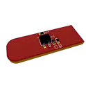
This is a QRE1113 opto-reflective sensor module, using a 47K pull-up resistor (R2) and a 100 Ohm resistor (R1). It includes a 1µF capacitor (C1) for stability and attaches to a JST connector (J1) for easy interfacing. Power is provided via VCC, with the output signal (OPTO_OUT) fed back. #OpticalSensor #industrialSensing #reusable #module #industrialsensing #onsemi #sublayout... show more61 Uses
1 Star
TC2030-CTX-NL
6-Pin \"No Legs\" Cable with 10-pin micro-connector for Cortex processors Cable assembly, designed for ARM Cortex® SWD debugging and programming, featuring a 6-pin Tag-Connect™ Plug-of-Nails™ connector that mates with the TC2030 target footprint and a 10-pin FTSH-105 compatible ribbon connector. The cable supports SWD signals including VCC, SWDIO/TMS, SWCLK/TCK, SWO/TDO, nRESET, and GND for direct connection between compatible debuggers and target PCBs. #CableAssembly #DebugCable #ARMCortex #SWD #TagConnect #TC2030 #ProgrammingCable... show more35 Uses
0 Stars
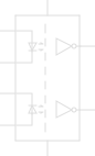
HCPL-063A
Dual High Speed HCMOS/LSTTL/TTL Compatible Optocoupler, dV/dt 1000/us, VCM 50, -0.5V to 7V VCC, SOIC-8 High speed optically coupled gates SOIC*3.9x4.9mm?P1.27mm*... show more8 Uses
0 Stars

DS1307Z+
64 x 8, Serial, I2C Real-time clock, 4.5V to 5.5V VCC, 0°C to +70°C, SOIC-8 RTC, I2C Timekeeping Chip SOIC*3.9x4.9mm?P1.27mm*... show more4 Uses
0 Stars

HR1204GY-P
High-Performance Digital PFC + Analog LLC Combo Controller with Standby Power Input to VCC #ultralibrarian... show more0 Uses
0 Stars

DS1302+
Trickle-Charge Timekeeping Chip, 2.0V to 5.5V VCC, 0°C to +70°C, DIP-8 RTC, Trickle-Charge Timekeeping Chip DIP*W7.62mm*... show more1 Use
0 Stars
SN74LVC11APWRQ1
AND Gate IC 3 Channel 14-TSSOP Triple 3-Input AND Gate that implements three independent positive-logic 3-input AND functions (Y = A × B × C). It operates from a 1.1 V to 3.6 V supply, features 5.5 V tolerant inputs, supports up to ±24 mA output drive (depending on VCC), and is specified for an operating temperature range of −40°C to +125°C. #TexasInstruments #LogicIC #ANDGate #TripleANDGate #SN74LVC11A #LVCLogic #DigitalLogic #AutomotiveElectronics #AECQ100 #TSSOP14... show more8 Uses
0 Stars

ESP-PSRAM32
32 Mbit serial pseudo SRAM device organized as 4Mx8 bits, 1.8 VCC, SOIC8 (SOP8) 32 Mbit serial pseudo SRAM MEMORY SOIC*3.9x4.9mm?P1.27mm*... show more5 Uses
0 Stars
74HC238N
3-to-8 line decoder/demultiplexer The 74HC238; 74HCT238 decodes three binary weighted address inputs (A0, A1 and A2) to eight mutually exclusive outputs (Y0 to Y7). The device features three enable inputs (E1 and E2 and E3). Every output will be LOW unless E1 and E2 are LOW and E3 is HIGH. This multiple enable function allows easy parallel expansion to a 1-of-32 (5 to 32 lines) decoder with just four '238 ICs and one inverter. The '238 can be used as an eight output demultiplexer by using one of the active LOW enable inputs as the data input and the remaining enable inputs as strobes. Inputs include clamp diodes. This enables the use of current limiting resistors to interface inputs to voltages in excess of VCC. • Wide supply voltage range from 2.0 to 6.0 V • CMOS low power dissipation • High noise immunity • Demultiplexing capability • Multiple input enable for easy expansion • Ideal for memory chip select decoding • Active HIGH mutually exclusive outputs • Input levels: • For 74HC238: CMOS level • For 74HCT238: TTL level • Complies with JEDEC standards • JESD8C (2.7 V to 3.6 V) • JESD7A (2.0 V to 6.0 V) • Latch-up performance exceeds 100 mA per JESD 78 Class II Level B • ESD protection: • HBM: ANSI/ESDA/JEDEC JS-001 class 2 exceeds 2000 V • CDM: ANSI/ESDA/JEDEC JS-002 class C3 exceeds 1000 V • Multiple package options • Specified from -40 °C to +85 °C and from -40 °C to +125 °C #74HC238N #74HCSeries #CMOSLogic #DecoderIC #Demultiplexer #DigitalLogic #AddressDecoder #ChipSelect #LogicGate #IntegratedCircuit #ElectronicsDesign #EmbeddedSystems... show more2 Uses
0 Stars





Page 1 of 3
Next