Chat
Welcome to Flux
Treat Flux like your intern. Tell it what you'd like to build and it'll get to work. You can also ask it questions, brainstorm ideas, and teach it your preferences. Learn More
Explain project
Write a project description
Find schematic issues
Create a test plan
Simulate a circuit
Prepare for Manufacturing
Component Selection Workflow
New Subsystem Wizard
Write I2C initialization code
Generate firmware skeleton
please explain what MK1 does.

@copilot please explain what MK1 does.
1y
The component $MK1$ in your project is a microphone, specifically the Knowles $SPH0645LM4H-B$. This microphone is a digital MEMS (Micro-Electro-Mechanical Systems) microphone with the following key features:
- Interface: I2S (Inter-IC Sound), a standard for digital audio communication.
- Voltage Supply (VDD): Connects to 3.3V in your schematic.
- Output: Provides digital output (DATA_OUT) that can be used by the ESP32 for processing.
- Other Pins:
- WS (Word Select): Used for channel selection in I2S, it defines left-right data frame division.
- BCLK (Bit Clock): Provides a clock signal for the serial communication.
- SELECT: Selects among different data formats or functionalities.
In your circuit, $MK1$ connects to the ESP32 for audio input, which probably allows your device to capture audio for processing or communication functions. Would you like to know how it's connected in this schematic?
1y
2
please explain what U2 does.
@copilot please explain what U2 does.
1y
The component U2 is an AMS1117-3.3, which is a voltage regulator. Specifically, it is a linear voltage regulator that takes a higher input voltage and reduces it to a steady 3.3V output.
Here’s how it operates in your circuit:
-
Input Voltage VIN: The input pin receives a higher input voltage that you want to regulate down to 3.3V. In your project, it's connected to the net
Net 12, which might be around 5V. -
Output Voltage VOUT and TAB(VOUT): These are output pins providing a regulated 3.3V, which powers various components in your circuit. They are connected to the 3.3V net in your circuit, denoted as
Net 1. -
Ground (GND): This pin is used to complete the circuit and is connected to the common ground net
GND.
The AMS1117-3.3 is used to ensure that sensitive components requiring 3.3V receive a stable and precise voltage supply regardless of fluctuations in the input voltage.
1y
1
please explain what J1 does.
@copilot please explain what J1 does.
1y
The component J1 is a USB Type-C connector, specified with the part number TYPE-C-31-M-12. This connector is typically used to provide power and data connections in electronic circuits.
Here are its pin functions and connections within your project:
- CC1 (Pins 1 and 11): Used for configuration channel signaling, it is connected to Net 16.
- DP1 and DP2 (Pins 2 and 12): Differential pair for USB data, connected to Net 14.
- DN1 and DN2 (Pins 3 and 13): Differential pair for USB data, connected to Net 15.
- SBU1 and SBU2 (Pins 4 and 14): Sideband use pins, not explicitly connected in the project.
- SHIELD (Pins 5, 6, 9, 10): Shield connections for grounding and electromagnetic protection.
- GND (Pins 7 and 8): Ground connections, part of the GND net.
- VBUS (Pins 15 and 16): Power lines providing voltage, connected to Net 13.
In this design, J1 primarily provides a power supply to the board through the VBUS line and serves as a USB data interface via DP and DN pins for communication.
1y
4
No files yet
Reviews
Documents
Documents are markdown text files which describe project goals, capture details, or even simulation outputs.
Assets

Kitchen Assistant Reference Design.png
Kitchen Assistant Reference DesignThumbnailAUIDO-Helper
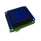
This is a Kitchen Assistant Reference Design that runs on an ESP32 that connects to the network. The board has a microphone and bazer for communication and a display
#referenceDesign #edge-computing #edgeComputing #espressif #template #esp32 #iot #i2s #reference-design
Properties
Pricing & Availability
Distributor | Qty 1 |
|---|---|
Arrow | $0.86–$1.07 |
Digi-Key | $1.07–$38.54 |
LCSC | $1.87–$2.24 |
Mouser | $1.58 |
Verical | $0.87–$1.24 |
Controls
Welcome 👋
Flux helps you build PCBs faster with an AI teammate!
Create your account to collaborate, stay updated, fork your own version, and get instant answers from our AI agent.
nawabusamabhatti
copilot
SSD1327, which indicates it is an OLED display driver IC. This component is likely responsible for driving an OLED display module.SSD1327display driver IC to an OLED display. It handles the interface with the MCU to display graphics, text, or other data on the connected OLED panel. If you need further help on how to connect it to the other components, feel free to ask!