Chat
Welcome to Flux
Treat Flux like your intern. Tell it what you'd like to build and it'll get to work. You can also ask it questions, brainstorm ideas, and teach it your preferences. Learn More
Explain project
Write a project description
Find schematic issues
Create a test plan
Simulate a circuit
Prepare for Manufacturing
Component Selection Workflow
New Subsystem Wizard
Write I2C initialization code
Generate firmware skeleton
New Comment
Someone is typing...
10
hi copilot

Someone is typing...
5
this link includes an electrical block diagram. Please review the block diagram ...
Someone is typing...
2
https://i.imgur.com/ofuFfS3.png
Someone is typing...
4
please compare this block diagram to my circuit and let me know if there's any d...
2y
Let's compare the block diagram provided in the image to your circuit:
-
Battery (LiPo), Solar (4V - 6V), and Power Management:
- Your design has provisions for solar power input VSOLAR (J3) and battery VBAT (J1). It also includes a battery charging IC (U2: CN3063) and a battery protection circuit. This matches the block diagram.
-
Voltage Regulator Circuit:
- Voltage regulation is handled by at least two devices on your schematic: U1 (RT8059GJ5) and U3 (SY6280AAAC), which corresponds to the block diagram.
-
Boost Converter:
- IC1 (MT3608L) is used as a boost converter in your project, which correlates with the block diagram.
-
Switch:
- The switch concept in the block diagram translates to SW1 and SW2 in your schematic, controlling different aspects of the circuit.
-
MCU (Microcontroller Unit):
- The MCU on your board is the XIAO RP2040 (U6), which is the microcontroller block in the diagram.
-
LoRa Module:
- The LoRa module is represented by U4 (LoRa-E5), aligning with the block diagram.
-
Connectors (I2C, RS485, UART):
- The RS485 interface is managed by IC2 (SP3485EN-L/TR). UART connections can be seen with pin designations of TX and RX from the MCU. I2C connections are present (SCL, SDA) to interface with external components, though specific external I2C devices are not detailed in the schematic description.
-
ESD (Electrostatic Discharge) Protection:
- ESD protection details aren't provided in your schematic description. It's essential to ensure there is proper ESD protection, especially on communication lines such as RS485, USB, and antenna connections.
-
RST (Reset) and BOOT:
- Designators for Reset and Boot (NRST and ENABLE) are present in your design, but their exact functionality and connections would need to be verified against the MCU's datasheet (U6) and the LoRa module (U4).
-
TX and RX LEDs:
- TX and RX activity can be indicated by D5 (Red LED) and D2 (Green LED). Ensure these are appropriately connected to indicate the transmission (TX) and reception (RX) activity as per the block diagram.
-
USB:
- There's a USB connection on the MCU (U6), which should correspond to a USB connection for communications or power on your physical board.
Overall, your circuit design seems to align well with the given block diagram. Ensure all connections, especially for the indicators (LEDs), ESD protection, and switch functionality, are correctly implemented as per functional requirements, and check proper component values and ratings to ensure reliable operation.
2y
Someone is typing...
13
this image contains a block diagram. Compare the diagram to my circuit and find ...

@copilot this image contains a block diagram. Compare the diagram to my circuit and find any differences  https://i.imgur.com/ofuFfS3.png
Image
2y
I will look for differences between the block diagram presented in the image and the textual description of your circuit. Let's analyze each segment provided in your schematic:
-
Power Input: The block diagram shows a power input section that can be either +12V or +5V. The schematic contains a solar input (VSOLAR) for power and battery input (VBAT), although the specific voltage levels for these are not mentioned in the text.
-
Boost Converter: The block diagram includes a boost converter, but your schematic does not specify a component with this exact function. However, it does include the MT3608L (Designator IC1) which is a boost converter IC.
-
Voltage Regulator: Your schematic includes the U1 (RT8059GJ5), which is a voltage regulator corresponding to the "Voltage Regulator circuit" in the block diagram.
-
Battery Protection and Charging: You have a U2 (CN3063), which is a charging IC and seems to have battery protection functions, attributing to both "Battery Charging IC" and "Battery Protection IC" in the block diagram.
-
Battery: The textual description of your schematic does not mention the type of battery used (like LiPo), just the designation VBAT.
-
Solar: The block diagram specifies a solar input of 4-6V, while your schematic simply mentions solar input (VSOLAR) without specifying voltage.
-
MCU: Your schematic specifies the use of the XIAO RP2040 (U6), which corresponds to the MCU in the block diagram.
-
LoRa Module: The LoRa-E5 module (U4) in your schematic matches the "LoRa Module" in the block diagram.
-
Connectors: The block diagram lists I2C, RS485, and UART connectors. Your schematic contains designations for these interfaces, such as SDA and SCL for I2C, RO and DI for RS485 (through IC2 which is an SP3485EN-L/TR), and TX/RX for UART.
-
ESD Protection: There is a general ESD label in the block diagram. Your schematic does not explicitly mention ESD protection components, but proper design usually integrates these into connectors or lines susceptible to ESD.
-
Indicating LEDs: Your schematic includes D5 and D2, which are LEDs likely used for TX and RX indication, respectively.
-
Switch: The block diagram includes a switch between the boost converter and the voltage regulator, but the schematic does not make explicit mention of a switch component.
-
USB: Your schematic includes the USB input (VUSB) for power or data.
-
Reset and Boot: The RESET and BOOT functions mentioned in the block diagram could correspond to the NRST and ENABLE nets in your schematic, which are typically used for resetting the MCU and configuring bootloader or firmware upload modes.
-
Max 485: Your schematic has an IC2 (SP3485EN-L/TR) which is an RS485 transceiver, comparable to the MAX3485 component seen on the block diagram.
Overall, the main differences are:
- The specific battery type and voltage range are not mentioned in your schematic.
- The solar input voltage is unspecified in the schematic.
- There's no explicit mention of a switch component in your schematic that would correspond to the one shown in the block diagram between the boost converter and voltage regulator circuit.
- ESD protection is not explicitly detailed in the schematic.
The rest of the components in your schematic appear to correlate with the block diagram.
2y
Someone is typing...
11
can you check if my project correctly implements this block diagram?
https://i....
@copilot can you check if my project correctly implements this block diagram?
Image
2y
Something went wrong, sorry. Please try again.
2y
Someone is typing...
9
+3V3
J3
+3V3
+3V3
VSOLAR
VBAT
VBAT
+3V3
VBAT
+3V3
12_5V
VBAT
VSOLAR
VUSB
+3V3
C11
Capacitance
4u7 F
U6
C1
Capacitance
10uF
VUSB
A
PIO2
SDA
PIO2
A
C4
Capacitance
4u7 F
SCL
+3V3
C2
Capacitance
10uF
C3
Capacitance
100nF
C8
Not Recommended for New Designs
Capacitance
68pF
+3V3
RX
NRST
RO
B
B
RX
NRST
TX
SDA
C10
Capacitance
22uF
PIO1
DI
C9
Capacitance
100nF
ENABLE
SCL
TX
C12
Capacitance
100nF
C7
Capacitance
22uF
PIO1
DI
12_5V
C6
Capacitance
100nF
C5
Capacitance
10uF
RO
R15
Resistance
4k7 Ω
R9
Resistance
20kΩ
R16
Resistance
4k7 Ω
R11
Resistance
22 Ω
R14
Resistance
120 Ω
R8
Resistance
2kΩ
R7
Resistance
15kΩ
R6
Resistance
150kΩ
R1
Resistance
3kΩ
R2
Resistance
1k5 Ω
R17
Resistance
4k7 Ω
R10
Resistance
22 Ω
R4
Resistance
4k7
Ω
R13
Resistance
470 Ω
R3
Resistance
68kΩ
R5
Resistance
6k8 Ω
R18
Resistance
22 Ω
U3
IC1
L1
Inductance
10uH
SW2
U4
L2
Inductance
2u2 H
D1
IC2
J1
U2
D4
D5
Color
Red
SW1
D2
Color
Green
D3
J6
H2
H1
U1
J2
No files yet
Reviews
Documents
Documents are markdown text files which describe project goals, capture details, or even simulation outputs.
Assets
svg
flux logo.svg
flux logoDefault
image-removebg.png
image-removebgThumbnailThe Green Dot 2040E5 Board qbzZ
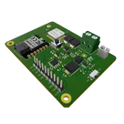
The "Green Dot 2040E5" Board is a Node that interfaces RS485 Sensor probes and can log information to the cloud using LoRa Connectivity. It uses the XIAO RP2040 and the LoRa-E5 (STM32WLE5JC) modules from Seeed Studio to do its magic. It also has amazing power management capabilities (Solar charging, Battery protection, etc) that make it very useful for IoT applications
#Seeed #XIOA #LoRa #RP2040 #IoT
Properties
Pricing & Availability
Distributor | Qty 1 |
|---|---|
Digi-Key | $6.46–$7.77 |
LCSC | $0.98–$1.55 |
Mouser | $8.40–$8.63 |
Controls
Welcome 👋
Flux helps you build PCBs faster with an AI teammate!
Create your account to collaborate, stay updated, fork your own version, and get instant answers from our AI agent.
kerry
Image
copilot