Chat
Welcome to Flux
Treat Flux like your intern. Tell it what you'd like to build and it'll get to work. You can also ask it questions, brainstorm ideas, and teach it your preferences. Learn More
Explain project
Write a project description
Find schematic issues
Create a test plan
Simulate a circuit
Prepare for Manufacturing
Component Selection Workflow
New Subsystem Wizard
Write I2C initialization code
Generate firmware skeleton
are there any unintended shorts in this schematic design?

2y
To assess the presence of unintended shorts in your schematic design, I've reviewed the connectivity and component arrangements based on the provided nets and connections. Here's a summary of key observations that could potentially involve unintended shorts, though without a full visual inspection or simulation, this analysis is based on common design considerations and the provided text description.
-
Common Ground and Power Nets:
- All components connected to the ground net (Net ID: 30971553804846619d1477578ea02688) and +3V3 power net seem appropriate and typical for ensuring that all parts of the circuit share a common reference point and have power supplied correctly.
-
Decoupling Capacitors:
- Decoupling capacitors (e.g., C1, C5, C6, etc.) are close to their respective power supply pins on integrated circuits, which is best practice. There's no indication that this would cause a short unless they are incorrectly placed across two different potentials that are not meant to be directly connected.
-
USB Differential Pairs:
- Resistors R3 and R6 are connected to the USB_DM and USB_DP lines, respectively (Nets: 6534a268e2e96958ea70d52fa9c2e80d and 355bb3652c10469f177df82d48430c44). Ensure these resistances match the requirements for USB impedance and that they are not shorting the differential pair but rather functioning within their expected role in the circuit.
-
Signal Lines to GPIOs:
- Various GPIOs are connected through nets to other components. These connections should be intentional and according to the functional requirements of your project (e.g., GPIO connections to LEDs, external modules, etc.). Ensure that each GPIO connection is intentional and does not create any unintended paths especially if certain pins are expected to be inputs or outputs which might conflict with external components' configurations.
-
Crystal Oscillator Connections:
- Ensure the crystal oscillator (connected through XIN and XOUT) and its loading capacitors (if any are used in your design not listed explicitly) are correctly connected to function without shorting the oscillator's output with any unintended part of the circuit.
-
SPI Flash Connections:
- The connections to the SPI flash (U3: W25Q128JVSIQ) including QSPI_CSN, QSPI_CLK, QSPI_SD0, etc., should be checked to ensure they match the SPI protocol without any unintended shorts between these communication lines. Pay special attention to the shared lines in SPI, ensuring each is only connected as intended.
Without explicit errors or conflicts cited in the nets list and without visual confirmation or EDA tool diagnostics, it's difficult to guarantee there are no unintended shorts. Please consider using design rule checks (DRC) and electrical rule checks (ERC) features within your EDA tool (like Flux) to automatically detect potential shorts or design conflicts. If you have specific concerns or areas you suspect might have issues, providing those details can help in giving a more targeted review.
2y
3
are there any unintended shorts in this schematic design?
2y
Reviewing your schematic to identify unintended shorts involves checking connections and ensuring that no two nets which should not be connected together are actually connected. Let’s go through some key points that could imply unintended shorts based on typical design guidelines and the details you've provided:
-
Power and Ground Nets: Ensure that power supply nets (+1V1, +3V3) and the ground net are not shorted to each other. This is the most common and critical check. Based on the nets detailed, there appears to be no direct indication of shorts between power and ground nets as they are described to connect to appropriate pins and components corresponding to their function.
-
Decoupling Capacitors: Should be connected between the power supply (VCC) pins of ICs and ground to provide local charge storage and noise filtering. Your list includes multiple decoupling capacitors (e.g., C1, C12, C17, etc.) seemingly correctly placed, without indication of shorts.
-
GPIOs and Signal Lines: GPIOs and other signal lines should only connect to their intended targets. For example, GPIO lines connected to LEDs, switches (SW2), or external interfaces must not be short-circuited to each other or to power/ground unless specifically intended. From the project details, each GPIO and signal line, like GPIO4, GPIO5, etc., seem correctly assigned to specific functions with no evident shorts.
-
Critical Net Checks:
- Power Nets $af60e7f4cb339d22ba3908b2f4f2d3c7$: Connects multiple VCC and 3.3V power supply pins across different components with decoupling capacitors correctly placed between VCC and GND, showing no unintended connections.
- Ground Nets $7cd815e0e9b888c42b1f87ad1e1a5c06$: Covers all GND connections across the components, including the decoupling capacitors and IC ground pins, without indicating any incorrect shorts to power or signal nets.
-
External Interfaces (USB, LoRa, QSPI), importantly, are correctly wired to their respective GPIOs or control lines, like D+, D-, RFIO, QSPI_SCLK, QSPI_SS, etc., with particular attention to ensure there’s no crossover or direct connection between these interfaces that could hint at an unintended short.
-
Specific Instructions in Notes: Notes mentioning specific proximity requirements (e.g., C11 close to pin 45 of RP2040), hint at critical design considerations but do not inherently suggest shorts.
-
LEDs and Resistors: The connections between GPIOs, LEDs (e.g., D1), and resistors (e.g., R2, R4, etc.) aim at current limiting and signal indication, with no evident shorts in their configurations.
Based on this high-level review, there are no apparent unintended shorts within your schematic as per the project description provided. However, it's essential to perform a thorough netlist check and possibly simulate the circuit or use a design rule check (DRC) feature within Flux to catch any less obvious issues. Also, ensuring that all component footprints match the intended schematic connections is key to avoiding physical shorts on the PCB.
2y
1
C13
Capacitance
100nF
C15
Capacitance
27pF
C9
Capacitance
100nF
C12
Capacitance
1uF
Note 7
U2
Note 3
C14
Capacitance
100nF
C11
Capacitance
1uF
C10
Capacitance
100nF
C3
Capacitance
100nF
C5
Capacitance
100nF
Note 5
C16
Capacitance
27pF
Extenal Flash
C17
Capacitance
100nF
C7
Capacitance
100nF
C8
Capacitance
100nF
Note 1
C2
Capacitance
100nF
Note 2
Note 6
Note 4
C4
Capacitance
100nF
C6
Capacitance
100nF
R7
Resistance
10kΩ
C1
Capacitance
4u7 F
R5
Resistance
1kΩ
U1
R6
Resistance
27.4 Ω
R3
Resistance
27.4 Ω
R2
Resistance
1k5 Ω
R4
Resistance
1kΩ
U3
J1
D1
Color
Green
SW2
No files yet
Reviews
Documents
Documents are markdown text files which describe project goals, capture details, or even simulation outputs.
Assets
board outline.svg
board outlineDefault
3D.png
3D
image-removebg-preview.png
image-removebg-previewThumbnailM.2 KeyB 2242 Card
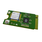
Welcome to your new project. Imagine what you can build here.
Properties
Properties describe core aspects of the project.
Pricing & Availability
Distributor | Qty 1 |
|---|---|
Digi-Key | $10.41–$10.70 |
LCSC | $31.45–$32.10 |
Mouser | $12.18 |
Controls
Welcome 👋
Flux helps you build PCBs faster with an AI teammate!
Create your account to collaborate, stay updated, fork your own version, and get instant answers from our AI agent.
kerry
copilot
Table