Single-Layer PCB Design for PICO
Thought for 59 sec
Guitar Instrument System Spec
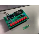
Board 2 - Internal core board
Power Architecture
Battery recommendation
Key Design Decisions
Main Risks
Recommended Next Step
A split-board guitar instrument with an external drum/control surface, an internal compute/audio core built around PICO plus a Raspberry Pi 4 Model B 4GB, optional distributed comms via a CAN Bus HAT, balanced audio through an XLR Connector, and power from a 1S Li-ion Battery Pack.
The right way to present this at your stage is as an architecture + power + signal-flow spec with clear subsystem boundaries and a block diagram, rather than diving straight into part-level wiring
Board Partition Board 1 - External control boardDiagram
Mounted on the guitar body exterior.
Table
| Function | Lives here | Notes |
|---|---|---|
| Drum sequencer controls | Yes | Active mainly in drum-edit mode |
| Capacitive touch modules | Yes | Keep local to reduce noise pickup |
| UI LEDs | Yes | Keep with user controls |
| Audio circuitry | No | Keep off this board |
| Main processing | No | No Raspberry Pi 4 Model B 4GB here |
Mounted in the body cavity.
Table
| Function | Lives here | Notes |
|---|---|---|
| PICO | Yes | Real-time control coprocessor |
| Raspberry Pi 4 Model B 4GB | Yes | Main synth, storage, sequencing, UI state |
| CAN Bus HAT | Yes | Attach on the Pi side |
| Power conversion | Yes | Battery, charge, 5 V, 3.3 V |
| Audio output stage | Yes | Keep close to XLR Connector |
| Rotary encoder with push | Wired here | Direct to PICO |
This subsystem-first structure is exactly the kind of architecture walkthrough recommended for explaining and defining a design before implementation
Compute Ownership
Raspberry Pi 4 Model B 4GB
Use it for:
- synth engine
- sample playback
- patch and file storage
- higher-level sequencing
- CAN application logic
- audio software stack
- system UI state
Use it for:
- rotary encoder decoding
- push-switch detection
- low-latency GPIO scanning
- receiving external control-board events
- forwarding clean events to the Pi
- fallback control logic during Pi boot
This split keeps timing-sensitive inputs local to the MCU and heavier compute/storage on the Pi, which matches good architecture grouping practice
Interconnect Definition
External control board PICO
Recommended minimum link:
Table
| Signal Group | Qty | Notes |
|---|---|---|
| 3.3 V | 1 | Logic power |
| GND | 2 | Use at least two returns |
| SDA / SCL or equivalent control bus | 2 | Preferred if modules support it |
| Interrupt / attention | 1 | Optional but useful |
| LED power or spare GPIO | 1-2 | Optional |
Target: 6 to 8 conductors
PICO Raspberry Pi 4 Model B 4GB
Preferred order:
- UART
- SPI if bandwidth needs increase
- USB only if you specifically want USB-device behavior
Keep standard HAT-side connectivity local on the core board.
Rotary Control Assignment
The rotary switch with push should stay directly on PICO.
That keeps quadrature decoding and debounce deterministic on the MCU side.
Audio Output
Use a balanced line output on an XLR Connector, not a speaker output.
Table
| Block | Recommendation |
|---|---|
| Audio source | Software/audio engine on Raspberry Pi 4 Model B 4GB |
| Output conditioning | Dedicated analog/balanced driver stage |
| Connector | XLR Connector on core board edge |
| Placement | Keep close to analog stage, far from touch/control routing |
Because the Raspberry Pi 4 Model B 4GB is in the system, the power tree matters more than anything else.
Recommended rails
Table
| Rail | Source | Powers |
|---|---|---|
| Battery | 1S Li-ion Battery Pack | Raw energy source |
| 5 V | Boost/regulation from battery path | Raspberry Pi 4 Model B 4GB, CAN Bus HAT, audio support as needed |
| 3.3 V | Regulated logic rail | PICO, control board logic, sensors/modules |
A single-cell 3.7 V rechargeable pack is a valid system battery concept, but it must feed:
- charge management
- protection
- a solid 5 V rail for the Pi
- a quiet 3.3 V rail for control logic
The project-explanation guidance specifically calls for defining input source, regulators, and rails early because they determine the whole system structure
Functional Modes
Table
| Mode | Active Elements |
|---|---|
| Boot | PICO alive first if possible, Pi starting |
| Drum edit | External control board + PICO + Pi sequencer logic |
| Synth/play mode | Pi audio engine + rotary control + selected UI |
| CAN mode | Pi + CAN Bus HAT + external node comms |
| Storage access | Pi-local storage only |
Table
| Decision | Why |
|---|---|
| Keep touch controls on a separate exterior board | Better isolation and simpler mechanics |
| Put rotary control on PICO | Better real-time handling |
| Let Pi own storage | Eliminates unnecessary third storage board |
| Keep audio and XLR Connector on core board | Better analog integrity |
| Keep CAN on Pi side | Simplifies system ownership |
Table
| Risk | Why it matters |
|---|---|
| 5 V power integrity | Pi stability depends on it |
| Ground noise into XLR path | Can ruin output quality |
| Long noisy control runs | Can hurt touch reliability |
| Too many raw inter-board signals | Makes wiring fragile and noisy |
The next engineering step should be:
- lock the power budget
- define the exact board connectors
- assign the PICO GPIO map
- decide whether the external board speaks I2C-style processed control or raw digital events
That sequence follows the general guidance to move from architecture into subsystem and interface definition before implementation detail
If you want, I can make the next version as a pin-budget table:
- external control board connector
- PICO pin assignments
- Raspberry Pi 4 Model B 4GB link choice
- power-rail ownership for each board.
Place components now
Run design review
Inspect board size


Welcome 👋
Flux helps you build PCBs faster with an AI teammate!
Create your account to collaborate, stay updated, fork your own version, and get instant answers from our AI agent.
kingzin
nolimit
nolimit
giulioz