Project Overview and Design Breakdown
1:00
Project
Accessed Knowledge (1)
Using Knowledge Base Tool.
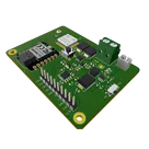
Here is a structured explanation of your “Green Dot 2040E5: Robust LoRa/RS485 IoT Node” project based on the current schematic.
1. Overall Purpose
This design is a robust, field-deployable IoT node for (likely outdoor) AgriTech use that can:
- Be powered from a Li-ion battery with solar input and USB for charging.
- Communicate wirelessly via LoRaWAN using a U4.
- Provide RS‑485 industrial bus connectivity using the IC2.
- Use a compact Seeed XIAO RP2040 module U6 as the main controller/host.
High-level: it is a flexible node that can talk long-range (LoRa) and wired bus (RS485), powered from a small solar‑charged battery.
2. Core Functional Blocks and How They Interact 2.1 Power Input and Battery/Charging
Sources and storage:
- Solar input via J3 (2‑Position Screw Terminal) on net VSOLAR:
- Goes through D1 (SS34) into the VIN node.
- USB power:
- Battery:
Interaction:
- Solar and USB power are OR’d with Schottky diodes (D1, D3) into VIN, avoiding back‑feeding between sources.
- U2 manages Li‑ion charging from VIN to VBAT, and reports charging states to LEDs via CHRG, DONE.
Trade-off:
- Diode OR-ing is simple and robust but wastes some headroom (diode drop).
- Dedicated power‑path management ICs could improve efficiency but are more complex/costly.
2.2 Main 3.3 V Rail
- 3.3 V regulator: U1.
Loads on +3V3:
- U6 (3V3 pin, SCL/SDA pins, UART pins).
- U4 on VCC.
- IC2 on VCC.
- C11, C12 and others provide decoupling on +3V3 and RS485 VCC.
Design choice:
- Using a switching converter from VBAT to 3.3 V (rather than a linear LDO) trades higher efficiency and better battery life against more EMI and design complexity.
2.3 Boost Converter for 12.5 V Rail
-
IC1 boost converter block:
-
- This allows selectable feedback configuration, likely to:
- Turn boost ON/OFF or
- Switch between different output voltages or operating modes.
- This allows selectable feedback configuration, likely to:
-
12.5 V appears on:
- 12_5V net, exported via a Net Portal and [J6](J6: Pin_10).
Use case:
- Powering external actuators, sensors, or valves that need ~12 V (very typical in irrigation and AgriTech).
Trade-offs:
- Boosting from VBAT (~3–4.2 V) to 12.5 V is inherently less efficient; only practical for low‑duty or low‑power loads.
- Adds complexity (inductor L1, diode D4, etc.) but increases node versatility.
2.4 MCU / Controller: Seeed XIAO RP2040
- U6 module:
- Powered from +3V3 (3V3 pin).
- Also has 5V / VUSB pin used as one of the power sources for the charger.
- IO connections:
- LoRa UART:
- Reset / control:
- RS485 logic:
- GPIO expansion:
Key technologies:
- RP2040 dual‑core MCU on a ready‑made module simplifies high‑speed design and flash/QSPI routing.
- The module includes USB, clock, and flash, so the baseboard is simpler.
Design choice:
- Using a pre‑built XIAO module trades BOM and per‑unit cost for:
- Faster development.
- Reduced risk around high‑speed layout and flash interfacing.
2.5 LoRa Radio: LoRa-E5 (STM32WLE5JC)
- U4:
- Powered from +3V3, decoupled to GND.
- RF output RFIO routed to J2 (IPEX1) for an external antenna.
- Control & data:
Trade-offs:
- LoRa‑E5 module is more expensive than discrete RF + MCU + matching, but:
- It massively reduces RF design risk.
- Simplifies certification and antenna matching.
2.6 RS-485 Interface
-
IC2 RS‑485 transceiver:
-
RS485 physical connector is the 10‑pin header J6, exposing:
- A, B, 3.3 V, GND, additional I/O (PIO1, PIO2), and 12.5 V.
Design choice:
- Using an RS‑485 transceiver instead of, say, RS‑232 or CAN leverages:
- Long cable operation.
- Robust noise immunity.
- Multi‑drop bus capability (common in agriculture, industrial fields).
2.7 User / Status Interfaces
- Charge status LEDs:
- DIP switch SW2 for LoRa/MCU mode selection via SW net to [U4](U4: PB13).
- SW1 SPDT for power/boost configuration (FB network).
- Mounting holes H1 and H2 for mechanical robustness.
- 3D enclosure notes 3D Enclosure and Enclosure suggesting a custom housing.
3. Design Choices, Trade-offs, and Optimizations Power Architecture
- Two DC‑DC stages: one for 3.3 V, one for 12.5 V.
- Optimized for battery efficiency and supporting higher‑voltage actuators.
- Diode OR-ing of solar and USB:
- Simple, rugged, but dissipates some power in the diodes.
- Single‑cell Li‑ion with U2:
- Common, high‑energy‑density chemistry.
- CN3063 gives a proven, integrated charger implementation.
- XIAO RP2040 module:
- Reduces design complexity; firmware‑friendly pinout.
- LoRa-E5 module:
- Pre‑certified RF and integrated STM32 simplifies radio and LoRaWAN stack.
- RS‑485 transceiver:
- Industrial‑grade long‑distance wired connectivity.
- Expansion header J6:
- Exposes power rails, RS‑485 bus, general IO, and boosted voltage for external modules/sensors.
- Multiple decoupling capacitors around each power IC and at distribution points.
- Differential RS‑485 with bias/termination resistors for bus stability.
- External antenna via IPEX for better LoRa range.
- Mechanical mounting holes and enclosure markers for real‑world deployment.
4. Functional Summary
Putting it all together:
- Solar panel and/or USB power feed the VIN rail via diodes.
- U2 charges the Li‑ion battery connected on VBAT and reports charge status on LEDs.
- From VBAT:
- The RP2040 module runs user firmware, managing:
- The node can be mounted in a custom enclosure and run autonomously in the field, solar‑charged and maintaining communication via LoRa and RS‑485.
If you want, next I can:
- Walk through just the power path step‑by‑step (VBAT/VIN/3V3/12.5V).
- Or focus on communication architecture (LoRa + RS‑485 + firmware implications).
Focus on power path
Check power sizing
LoRa + firmware details
Review RS485 section
Optimize for battery life
105 days
Ready.
I want you to optimize this micropython code for speed and low power consumption...
Perform a design review to verify that each passive component's voltage rating i...
11
with consideration of this project requirements, pin mapping and context, write ...
7
using references and pin description of U6 write a baremetal C/C++ driver that I...
9
write a comprehensive documenation of this code files provided with regards to t...
5
Perform a design review to ensure that all current limiting resistors in the sch...
13
simulate the output of this code with appropriate input values
import time
impo...
4
using references and pin description of U6 write a baremetal C/C++ driver that ...
8
I want to use this board to read temperature data from an I2C sensor and send th...
3
Perform a design review to verify that each passive component's voltage rating i...
12
Perform a design review to verify that each passive component's voltage rating i...
10
Perform Power Consumption Calculations to determine the total power consumption ...
14
Perform an Electrical Rule Check (ERC) on the schematic for all the ICs, specifi...
2
use python to recreate the graphs described in the datasheet of U1
15
+3V3
C11
Capacitance
4u7 F
U6
VUSB
R15
Resistance
4k7 Ω
R9
Resistance
20k Ω
A
R16
Resistance
4k7 Ω
R11
Resistance
22 Ω
R14
Resistance
120 Ω
PIO2
+3V3
+3V3
PIO2
R8
Resistance
2k Ω
R7
Resistance
15k Ω
R6
Resistance
150k Ω
A
+3V3
+3V3
+3V3
R1
Resistance
3k Ω
IC1
C2
Capacitance
10u F
L1
Inductance
10u H
VBAT
SW2
U4
ENABLE
IC2
R2
Resistance
1k5 Ω
C8
Not Recommended for New Designs
Capacitance
68p F
+3V3
R17
Resistance
4k7 Ω
RX
U2
NRST
D4
RO
R10
Resistance
22 Ω
R4
Resistance
4k7
Ω
R13
Resistance
470 Ω
B
B
RX
NRST
TX
+3V3
+3V3
D5
Color
Red
C10
Capacitance
22u F
PIO1
RX
DI
SW1
D2
Color
Green
+3V3
ENABLE
+3V3
12_5V
TX
C12
Capacitance
100n F
R3
Resistance
68k Ω
J2
PIO1
DI
12_5V
J6
H2
R5
Resistance
6k8 Ω
L2
Inductance
2u2 H
C6
Capacitance
100n F
H1
C5
Capacitance
10u F
R18
Resistance
22 Ω
RO
+3V3
U1
U3
Reviews

- Wirelessly connects nets on schematic. Used to organize schematics and separate functional blocks. To wirelessly connect net portals, give them same designator. #portaljharwinbarrozo43.0M
- Wirelessly connects power nets on schematic. Identical to the net portal, but with a power symbol. Used to organize schematics and separate functional blocks. To wirelessly connect power net portals, give them the same designator. #portal #powerjharwinbarrozo11.4M
- A generic fixed resistor for rapid developing circuit topology. Save precious design time by seamlessly add more information to this part (value, footprint, etc.) as it becomes available. Standard resistor values: 1.0Ω 10Ω 100Ω 1.0kΩ 10kΩ 100kΩ 1.0MΩ 1.1Ω 11Ω 110Ω 1.1kΩ 11kΩ 110kΩ 1.1MΩ 1.2Ω 12Ω 120Ω 1.2kΩ 12kΩ 120kΩ 1.2MΩ 1.3Ω 13Ω 130Ω 1.3kΩ 13kΩ 130kΩ 1.3MΩ 1.5Ω 15Ω 150Ω 1.5kΩ 15kΩ 150kΩ 1.5MΩ 1.6Ω 16Ω 160Ω 1.6kΩ 16kΩ 160kΩ 1.6MΩ 1.8Ω 18Ω 180Ω 1.8KΩ 18kΩ 180kΩ 1.8MΩ 2.0Ω 20Ω 200Ω 2.0kΩ 20kΩ 200kΩ 2.0MΩ 2.2Ω 22Ω 220Ω 2.2kΩ 22kΩ 220kΩ 2.2MΩ 2.4Ω 24Ω 240Ω 2.4kΩ 24kΩ 240kΩ 2.4MΩ 2.7Ω 27Ω 270Ω 2.7kΩ 27kΩ 270kΩ 2.7MΩ 3.0Ω 30Ω 300Ω 3.0KΩ 30KΩ 300KΩ 3.0MΩ 3.3Ω 33Ω 330Ω 3.3kΩ 33kΩ 330kΩ 3.3MΩ 3.6Ω 36Ω 360Ω 3.6kΩ 36kΩ 360kΩ 3.6MΩ 3.9Ω 39Ω 390Ω 3.9kΩ 39kΩ 390kΩ 3.9MΩ 4.3Ω 43Ω 430Ω 4.3kΩ 43KΩ 430KΩ 4.3MΩ 4.7Ω 47Ω 470Ω 4.7kΩ 47kΩ 470kΩ 4.7MΩ 5.1Ω 51Ω 510Ω 5.1kΩ 51kΩ 510kΩ 5.1MΩ 5.6Ω 56Ω 560Ω 5.6kΩ 56kΩ 560kΩ 5.6MΩ 6.2Ω 62Ω 620Ω 6.2kΩ 62KΩ 620KΩ 6.2MΩ 6.8Ω 68Ω 680Ω 6.8kΩ 68kΩ 680kΩ 6.8MΩ 7.5Ω 75Ω 750Ω 7.5kΩ 75kΩ 750kΩ 7.5MΩ 8.2Ω 82Ω 820Ω 8.2kΩ 82kΩ 820kΩ 8.2MΩ 9.1Ω 91Ω 910Ω 9.1kΩ 91kΩ 910kΩ 9.1MΩ #generics #CommonPartsLibraryjharwinbarrozo1.5M
- A generic fixed capacitor ideal for rapid circuit topology development. You can choose between polarized and non-polarized types, its symbol and the footprint will automatically adapt based on your selection. Supported options include standard SMD sizes for ceramic capacitors (e.g., 0402, 0603, 0805), SMD sizes for aluminum electrolytic capacitors, and through-hole footprints for polarized capacitors. Save precious design time by seamlessly add more information to this part (value, footprint, etc.) as it becomes available. Standard capacitor values: 1.0pF 10pF 100pF 1000pF 0.01uF 0.1uF 1.0uF 10uF 100uF 1000uF 10,000uF 1.1pF 11pF 110pF 1100pF 1.2pF 12pF 120pF 1200pF 1.3pF 13pF 130pF 1300pF 1.5pF 15pF 150pF 1500pF 0.015uF 0.15uF 1.5uF 15uF 150uF 1500uF 1.6pF 16pF 160pF 1600pF 1.8pF 18pF 180pF 1800pF 2.0pF 20pF 200pF 2000pF 2.2pF 22pF 20pF 2200pF 0.022uF 0.22uF 2.2uF 22uF 220uF 2200uF 2.4pF 24pF 240pF 2400pF 2.7pF 27pF 270pF 2700pF 3.0pF 30pF 300pF 3000pF 3.3pF 33pF 330pF 3300pF 0.033uF 0.33uF 3.3uF 33uF 330uF 3300uF 3.6pF 36pF 360pF 3600pF 3.9pF 39pF 390pF 3900pF 4.3pF 43pF 430pF 4300pF 4.7pF 47pF 470pF 4700pF 0.047uF 0.47uF 4.7uF 47uF 470uF 4700uF 5.1pF 51pF 510pF 5100pF 5.6pF 56pF 560pF 5600pF 6.2pF 62pF 620pF 6200pF 6.8pF 68pF 680pF 6800pF 0.068uF 0.68uF 6.8uF 68uF 680uF 6800uF 7.5pF 75pF 750pF 7500pF 8.2pF 82pF 820pF 8200pF 9.1pF 91pF 910pF 9100pF #generics #CommonPartsLibraryjharwinbarrozo1.5M
- A generic fixed inductor for rapid developing circuit topology. *You can now change the footprint and 3D model at the top level anytime you want. This is the power of #genericsjharwinbarrozo15.5k
- An electrical connector acting as reusable interface to a conductor and creating a point where external circuits can be connected.Terminal
- 47 kOhms ±5% 0.125W, 1/8W Chip Resistor 0805 (2012 Metric) Automotive AEC-Q200 Thick Film #forLedBlinkjharwinbarrozo1.2M
- 10uF Capacitor Aluminum Polymer 20% 16V SMD 5x5.3mm #forLedBlink #commonpartslibrary #capacitor #aluminumpolymer #radialcanjharwinbarrozo1.2M
- Yellow 595nm LED Indication - Discrete 1.7V 1206 (3216 Metric) #forLedBlinkjharwinbarrozo1.1M


Welcome 👋
Flux helps you build PCBs faster with an AI teammate!
Create your account to collaborate, stay updated, fork your own version, and get instant answers from our AI agent.