Block Diagram Creation指导
Thought for 1 min 19 sec
55 days
Je ne peux pas corriger le schéma à partir de ce lien seul.
La page que tu as envoyée renvoie surtout vers une page de recherche/vidéo MathWorks, et le contenu récupérable ici ne montre pas le diagramme lui-même ni les éléments à corriger. Je ne peux donc pas déduire de façon fiable quelles erreurs tu veux que je rectifie.
Envoie-moi plutôt l’un de ces 2 éléments :
- une capture du diagramme à corriger
- ou la liste exacte des erreurs
Par exemple :
- mauvais ordre des blocs
- rails 3.3 V / 5 V / 12 V faux
- flèches dans le mauvais sens
- blocs manquants
- libellés incorrects
- style trop chargé
Si tu veux, colle simplement l’image ici et je te renverrai une version corrigée propre.
Open the link
Key steps only
PCB-relevant takeaways
can you help me add to my schematic dusk to dawn 5v out using mosfet and npn
Someone is typing...
23
how can i connect u1 and u4
Someone is typing...
8
Iset = 6800 / Rset
Iset = 6800 / 6.8k
Iset = 1A
Someone is typing...
3
Generate a markdown-formatted table to compare D5, D2. Highlight the main differ...
Someone is typing...
10
using the correct mermaid syntax, create a high level mermaid block diagram of t...
Someone is typing...
5
explain this project.
Someone is typing...
17
explain this project.
Someone is typing...
17
using current configurations, what is the charging current?
Someone is typing...
9
create a high level mermaid block diagram of IC1. Include key component's manufa...
Someone is typing...
28
please explain what U4 does.
Someone is typing...
22
create a detailed step by step plan table for this project to verify its functio...
Someone is typing...
12
list all R6 pins in a table format. For each pin provide its pin number, pin nam...
Someone is typing...
27
what's is ic1
Someone is typing...
25
C10? PART NO
Someone is typing...
30
WHAT IS THIS PROJECG ABOUT
Someone is typing...
21
Outline the electrical characteristics of U4 as detailed in the datasheet. Then,...
Someone is typing...
15
Perform an Electrical Rule Check (ERC) on the schematic for all the ICs, specifi...
Someone is typing...
7
create a high level mermaid block diagram of R7. Include key component's manufac...
Someone is typing...
13
create a high level mermaid block diagram of this project. Include key component...
Someone is typing...
4
, please perform a Design for Testability (DFT) review on the current schematic....
Someone is typing...
6
how do I change 12v out from boost to 5v
Someone is typing...
26
I\_ch = (V\_set / R\_set) x 900
I\_ch = (2 / 2k) x 900
I\_ch = 900mA
Someone is typing...
2
burada neden 10uH kullanılmış
Someone is typing...
14
explain this project.
Someone is typing...
16
MOUNTINT HOLE DIMENTIONS
Someone is typing...
31
Please validate the component ratings against the specified design parameters. T...
Someone is typing...
11
please explain what L1 does.
Someone is typing...
20
explain this project.
Someone is typing...
17
J3
C1
Capacitance
10uF
R9
Resistance
20kΩ
R8
Resistance
2kΩ
U3
Manufacturer Part Number
SY6280A AC
R7
Resistance
15kΩ
R6
Resistance
150kΩ
U1
Manufacturer Part Number
RT8059GJ5
C4
Capacitance
4u7 F
R1
Resistance
3kΩ
IC1
C2
Capacitance
10uF
U4
C3
Capacitance
100nF
L1
Inductance
10uH
SETTING OUTPUT VOLTAGE
Line 1
------------------------------------------------------------
Line 2
The internal reference VREF is typically 0.6V.
The output voltage is divided by a resistor divider,R1 and R2 to the FB pin.
Line 3
Vout = Vref x (1 + R6/R9)
Line 4
------------------------- AND ---------------------------
Line 5
Vout = Vref x (1 + R6/(R1+R4))
D1
R2
Resistance
1k5 Ω
C8
Capacitance
68pF
VSOLAR
VUSB
VBAT
+3V3
D4
R4
Resistance
4k7
Ω
VBAT
VBAT
C10
Capacitance
22uF
C9
Capacitance
100nF
+3V3
12_5V
R3
Resistance
68kΩ
C7
Capacitance
22uF
VBAT
VSOLAR
D3
R5
Resistance
6k8 Ω
VUSB
L2
Inductance
2u2 H
C6
Capacitance
100nF
C5
Capacitance
10uF
12_5V
J1
D5
Color
Red
SW1
D2
Color
Green
J4
J2
Reviews
 A generic fixed inductor suitable for rapid circuit topology development. The footprint automatically adapts based on the selected package, supporting standard SMD sizes (e.g., 0402, 0603, 0805) as well as well-known inductor packages such as SDR1806, PA4320, SRN6028, and SRR1260. Standard inductor values: 1.0 nH, 10 nH, 100 nH, 1.0 µH, 10 µH, 100 µH, 1.0 mH 1.2 nH, 12 nH, 120 nH, 1.2 µH, 12 µH, 120 µH, 1.2 mH 1.5 nH, 15 nH, 150 nH, 1.5 µH, 15 µH, 150 µH, 1.5 mH 1.8 nH, 18 nH, 180 nH, 1.8 µH, 18 µH, 180 µH, 1.8 mH 2.2 nH, 22 nH, 220 nH, 2.2 µH, 22 µH, 220 µH, 2.2 mH 2.7 nH, 27 nH, 270 nH, 2.7 µH, 27 µH, 270 µH, 2.7 mH 3.3 nH, 33 nH, 330 nH, 3.3 µH, 33 µH, 330 µH, 3.3 mH 3.9 nH, 39 nH, 390 nH, 3.9 µH, 39 µH, 390 µH, 3.9 mH 4.7 nH, 47 nH, 470 nH, 4.7 µH, 47 µH, 470 µH, 4.7 mH 5.6 nH, 56 nH, 560 nH, 5.6 µH, 56 µH, 560 µH, 5.6 mH 6.8 nH, 68 nH, 680 nH, 6.8 µH, 68 µH, 680 µH, 6.8 mH 8.2 nH, 82 nH, 820 nH, 8.2 µH, 82 µH, 820 µH, 8.2 mH #generics #CommonPartsLibraryjharwinbarrozo16.2k
- A generic fixed capacitor ideal for rapid circuit topology development. You can choose between polarized and non-polarized types, its symbol and the footprint will automatically adapt based on your selection. Supported options include standard SMD sizes for ceramic capacitors (e.g., 0402, 0603, 0805), SMD sizes for aluminum electrolytic capacitors, and through-hole footprints for polarized capacitors. Save precious design time by seamlessly add more information to this part (value, footprint, etc.) as it becomes available. Standard capacitor values: 1.0pF, 10pF, 100pF, 1000pF, 0.01uF, 0.1uF, 1.0uF, 10uF, 100uF, 1000uF, 10000uF 1.1pF, 11pF, 110pF, 1100pF 1.2pF, 12pF, 120pF, 1200pF 1.3pF, 13pF, 130pF, 1300pF 1.5pF, 15pF, 150pF, 1500pF, 0.015uF, 0.15uF, 1.5uF, 15uF, 150uF, 1500uF 1.6pF, 16pF, 160pF, 1600pF 1.8pF, 18pF, 180pF, 1800pF 2.0pF, 20pF, 200pF, 2000pF 2.2pF, 22pF, 220pF, 2200pF, 0.022uF, 0.22uF, 2.2uF, 22uF, 220uF, 2200uF 2.4pF, 24pF, 240pF, 2400pF 2.7pF, 27pF, 270pF, 2700pF 3.0pF, 30pF, 300pF, 3000pF 3.3pF, 33pF, 330pF, 3300pF, 0.033uF, 0.33uF, 3.3uF, 33uF, 330uF, 3300uF 3.6pF, 36pF, 360pF, 3600pF 3.9pF, 39pF, 390pF, 3900pF 4.3pF, 43pF, 430pF, 4300pF 4.7pF, 47pF, 470pF, 4700pF, 0.047uF, 0.47uF, 4.7uF, 47uF, 470uF, 4700uF 5.1pF, 51pF, 510pF, 5100pF 5.6pF, 56pF, 560pF, 5600pF 6.2pF, 62pF, 620pF, 6200pF 6.8pF, 68pF, 680pF, 6800pF, 0.068uF, 0.68uF, 6.8uF, 68uF, 680uF, 6800uF 7.5pF, 75pF, 750pF, 7500pF 8.2pF, 82pF, 820pF, 8200pF 9.1pF, 91pF, 910pF, 9100pF #generics #CommonPartsLibraryjharwinbarrozo1.5M
- A generic fixed resistor ideal for rapid circuit topology development. Its footprint automatically adapts based on the selected package case code—supporting 0402, 0603, 0805, 1203, and many other standard SMD packages, as well as axial horizontal and vertical configurations. Save precious design time by seamlessly add more information to this part (value, footprint, etc.) as it becomes available. Standard resistor values: 1.0 ohm, 10 ohm, 100 ohm, 1.0k ohm, 10k ohm, 100k ohm, 1.0M ohm 1.1 ohm, 11 ohm, 110 ohm, 1.1k ohm, 11k ohm, 110k ohm, 1.1M ohm 1.2 ohm, 12 ohm, 120 ohm, 1.2k ohm, 12k ohm, 120k ohm, 1.2M ohm 1.3 ohm, 13 ohm, 130 ohm, 1.3k ohm, 13k ohm, 130k ohm, 1.3M ohm 1.5 ohm, 15 ohm, 150 ohm, 1.5k ohm, 15k ohm, 150k ohm, 1.5M ohm 1.6 ohm, 16 ohm, 160 ohm, 1.6k ohm, 16k ohm, 160k ohm, 1.6M ohm 1.8 ohm, 18 ohm, 180 ohm, 1.8K ohm, 18k ohm, 180k ohm, 1.8M ohm 2.0 ohm, 20 ohm, 200 ohm, 2.0k ohm, 20k ohm, 200k ohm, 2.0M ohm 2.2 ohm, 22 ohm, 220 ohm, 2.2k ohm, 22k ohm, 220k ohm, 2.2M ohm 2.4 ohm, 24 ohm, 240 ohm, 2.4k ohm, 24k ohm, 240k ohm, 2.4M ohm 2.7 ohm, 27 ohm, 270 ohm, 2.7k ohm, 27k ohm, 270k ohm, 2.7M ohm 3.0 ohm, 30 ohm, 300 ohm, 3.0K ohm, 30K ohm, 300K ohm, 3.0M ohm 3.3 ohm, 33 ohm, 330 ohm, 3.3k ohm, 33k ohm, 330k ohm, 3.3M ohm 3.6 ohm, 36 ohm, 360 ohm, 3.6k ohm, 36k ohm, 360k ohm, 3.6M ohm 3.9 ohm, 39 ohm, 390 ohm, 3.9k ohm, 39k ohm, 390k ohm, 3.9M ohm 4.3 ohm, 43 ohm, 430 ohm, 4.3k ohm, 43K ohm, 430K ohm, 4.3M ohm 4.7 ohm, 47 ohm, 470 ohm, 4.7k ohm, 47k ohm, 470k ohm, 4.7M ohm 5.1 ohm, 51 ohm, 510 ohm, 5.1k ohm, 51k ohm, 510k ohm, 5.1M ohm 5.6 ohm, 56 ohm, 560 ohm, 5.6k ohm, 56k ohm, 560k ohm, 5.6M ohm 6.2 ohm, 62 ohm, 620 ohm, 6.2k ohm, 62K ohm, 620K ohm, 6.2M ohm 6.8 ohm, 68 ohm, 680 ohm, 6.8k ohm, 68k ohm, 680k ohm, 6.8M ohm 7.5 ohm, 75 ohm, 750 ohm, 7.5k ohm, 75k ohm, 750k ohm, 7.5M ohm 8.2 ohm, 82 ohm, 820 ohm, 8.2k ohm, 82k ohm, 820k ohm, 8.2M ohm 9.1 ohm, 91 ohm, 910 ohm, 9.1k ohm, 91k ohm, 910k ohm, 9.1M ohm #generics #CommonPartsLibraryjharwinbarrozo1.5M
- An electrical connector acting as reusable interface to a conductor and creating a point where external circuits can be connected.Terminal
- Wirelessly connects nets on schematic. Used to organize schematics and separate functional blocks. To wirelessly connect net portals, give them same designator. #portaljharwinbarrozo43.0M
- General Purpose Thick Film Standard Power and High-Power Chip Resistor 47 kOhms ±5% 0.125W, 1/8W Chip Resistor 0805 (2012 Metric) Automotive AEC-Q200 Thick Film Features: - RMCF – standard power ratings - RMCP – high power ratings - Nickel barrier terminations standard - Power derating from 100% at 70ºC to zero at +155ºC - RoHS compliant, REACH compliant, and halogen free - AEC-Q200 compliantjharwinbarrozo1.2M
- 10 µF 16 V Aluminum - Polymer Capacitors Radial, Can - SMD 30mOhm 2000 Hrs @ 105°C #commonpartslibrary #capacitor #aluminumpolymer #radialcanjharwinbarrozo1.2M
- Battery Holder (Open) Coin, 20.0mm 1 Cell SMD (SMT) Tab bate or batt #forLedBlinkjharwinbarrozo700.5k


BRAVE POWER MANAGEMENT BOARD
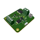
Brave is a versatile and efficient power board that can provide 12v, 5v and 3.3v outputs for various applications. It can be powered by battery or solar panel, and the battery can be recharged by solar energy. It can also be powered by a USB port if needed. This board is ideal for IoT projects that require reliable and stable power supply in different environments. #internetOfThings
#IoT #power #management #usb
Properties
Properties describe core aspects of the project.
Pricing & Availability
Distributor | Qty 1 |
|---|---|
Arrow | $0.81–$2.17 |
Digi-Key | $0.73–$2.82 |
LCSC | $1.72–$2.90 |
Mouser | $3.10–$3.73 |
Verical | $0.48–$1.96 |
Controls
Welcome 👋
Flux helps you build PCBs faster with an AI teammate!
Create your account to collaborate, stay updated, fork your own version, and get instant answers from our AI agent.