Chat
Welcome to Flux
Treat Flux like your intern. Tell it what you'd like to build and it'll get to work. You can also ask it questions, brainstorm ideas, and teach it your preferences. Learn More
Explain this part
Write a part description
Describe each pin
Operating conditions
Electrical max ratings
Part Specifications
Application circuits
Verify Part Details
Recommend similar parts
Check availability & lifecycle
TXN1_P1
Pin Number
47
VP12_P3
Pin Number
3
TXP1_P1
Pin Number
48
PLED/FN_C
Pin Number
32
OVCURJ
Pin Number
33
DP_P2
Pin Number
63
RXN1_P0
Pin Number
41
RXP1_P0
Pin Number
42
TXN1_P2
Pin Number
56
TXN1_P0
Pin Number
38
DVDD12_2
Pin Number
55
DM_P2
Pin Number
64
TXP1_P4
Pin Number
12
TXP1_P3
Pin Number
2
DM_P0
Pin Number
36
AVDD33_2
Pin Number
35
TXP1_P0
Pin Number
39
P_SPI_DI
Pin Number
30
VP12_P2
Pin Number
58
SW
Pin Number
19
RTERM
Pin Number
16
RXN1_P4
Pin Number
14
PWRENJ
Pin Number
34
P_SPI_CZ
Pin Number
31
RXP1_P2
Pin Number
60
AVDD12
Pin Number
46
DP_P4
Pin Number
9
RXP1_P3
Pin Number
5
AVDD33_4
Pin Number
54
VP12_P1
Pin Number
49
DM_P1
Pin Number
53
TXN1_P4
Pin Number
11
VP12_P0
Pin Number
40
V33
Pin Number
21
RXN1_P1
Pin Number
50
P_SPI_CK
Pin Number
29
DP_P0
Pin Number
37
DP_P3
Pin Number
6
DP_P1
Pin Number
52
RXP1_P4
Pin Number
15
VDDP/V5
Pin Number
20
DVDD12_3
Pin Number
61
VP12_P4
Pin Number
13
DM_P4
Pin Number
10
RESETJ
Pin Number
24
TXP1_P2
Pin Number
57
X1
Pin Number
45
X2
Pin Number
44
FN_B
Pin Number
23
RXN1_P3
Pin Number
4
VSSP
Pin Number
18
FN_A
Pin Number
22
DM_P3
Pin Number
7
AVDD33_3
Pin Number
43
DVDD33_1
Pin Number
26
P_SPI_DO
Pin Number
28
TXN1_P3
Pin Number
1
DVDD33_2
Pin Number
62
FB
Pin Number
17
AVDD33_1
Pin Number
8
EP
Pin Number
65
VBUS
Pin Number
25
DVDD12_1
Pin Number
27
RXN1_P2
Pin Number
59
RXP1_P1
Pin Number
51
No files yet
Reviews

GL3510-OSY52
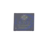
USB 3.1 QFN-64 Interface Controllers RoHS 4.75V5.25V,0+70,Channels 2
GL3510 is a low-power USB 3.1 Gen1 hub controller from Genesys Logic available in 2-port and 4-port configurations. It integrates USB 3.1 Gen1 SuperSpeed PHY and USB 2.0 High-Speed PHY, providing backward compatibility with USB 2.0 and USB 1.1 devices. The controller includes integrated 5V-to-3.3V and 5V-to-1.2V regulators, reducing external component count and PCB complexity. GL3510 supports USB Battery Charging Specification BC1.2, including Charging Downstream Port (CDP) and Dedicated Charging Port (DCP) modes, allowing fast charging of smartphones, tablets, and portable devices even during system sleep or power-off states. Suitable for USB hubs, docking stations, industrial computers, embedded systems, monitors, and consumer electronics.
Search Keywords:
GL3510, GL3510-52, Genesys Logic GL3510, USB 3.1 hub controller, USB hub IC, USB 3.1 Gen1 hub, SuperSpeed USB hub controller, USB 2.0 hub controller, 4-port USB hub, 2-port USB hub, USB BC1.2 controller, charging downstream port controller, dedicated charging port controller, USB docking station controller, embedded USB hub, USB expansion controller, USB host interface, QFN64 USB hub, QFN48 USB hub
GL3510
Properties
Pricing & Availability
No results found.
Controls
Welcome 👋
Flux accelerates your PCB design with AI.
Create your account to start using this component and bring your ideas to life.