Power Bank Design Overview
Thought for 2 mins 20 sec
Project Overview
1. Purpose and Real-World Applications
2. Core Components & Technologies
Key Technologies:
3. Block Diagram: Major Interactions
4. Design Breakdown & Implementation Steps 4.1 Schematic Structure
5. Key Design Choices, Trade-offs & Optimizations
6. Challenges & Performance Considerations
7. Scalability & Enhancement Opportunities
8. Summary Table: Main Design Elements
Final Notes
Title: Powerbank board
Purpose:
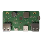
This project is a fully-integrated bi-directional USB Power Delivery (PD) 3.0 and fast-charge power bank supporting multiple input and output ports, based on the IP5328P system-on-chip (SOC).
Purpose:
This project is a fully-integrated bi-directional USB Power Delivery (PD) 3.0 and fast-charge power bank supporting multiple input and output ports, based on the IP5328P system-on-chip (SOC).
1. Purpose and Real-World Applications
- Mobile Power Solution: Provides portable battery-backed power both for charging devices (phones, tablets, accessories) and possibly for powering or charging itself via USB.
- Bi-directional Capability: Allows both charging from and supplying power to external devices using PD 3.0 and legacy USB protocols, making it compatible across a wide device ecosystem.
- Applications: Portable chargers, smart gadgets, IoT nodes, emergency backup batteries, or DIY battery-powered hubs.
2. Core Components & Technologies
Table
| Component | Type/Function |
|---|---|
| IP5328P | Main Power Bank SOC: Handles USB PD, battery mgt |
| J1 | USB Micro-B: Likely for charging input |
| J3, J4 | USB Type-A outputs for charging external devices |
| L1 | Main Power Inductor for switching regulator |
| C1-C20, CP1-CP14 | Bulk and decoupling capacitors: stabilize supplies |
| R1-R14, RNTC1 | Resistors: Feedback, pull-ups, NTC for battery temp |
| SW1 | User pushbutton: on/off or function select |
| Q1-Q4 | MOSFETs: Power/power path switching & protection |
| D1-D8 | LEDs: Charging/Status indication |
| J2 | USB-C/Custom (632723100011): Possible extra port |
| Net Portals [+ GNDs, etc.] | Board connectivity, signals, portals |
- USB Power Delivery (PD 3.0) Protocol
- Fast charging standards
- DC-DC switching conversion (buck-boost/etc.)
- Smart switch/MOSFET power path control
- Embedded microcontroller or logic within main SOC
3. Block Diagram: Major Interactions
Image
(Not a literal schematic, but a conceptual interaction flow)
4. Design Breakdown & Implementation Steps 4.1 Schematic Structure
- SOC (U1) is the core, interfacing with:
- Input: USB Micro-B (J1) and J2) can accept power to charge the internal battery (control via SOC and FETs).
- Switching Regulation: L1 inductor and associated passives enable high-efficiency DC-DC conversion for stepping voltages up/down as required (boost/buck/charge).
- Output: J3, J4 distribute power to external devices, with FETs (Q1-Q4) handling isolation and protection.
- User Input: SW1 allows human-initiated actions like power cycling, mode switching, or indication request.
- Indicators: LEDs (D1-D8) show status (charging, error, power state, etc.).
- Battery Management: Integrated NTC (RNTC1) for thermal protection, precision resistors for sensing.
- USB Signals: Data and configuration lines via net portals (CC1/CC2, D+/D-, etc.) are routed to the SOC for PD negotiation, legacy USB compatibility, and charge protocol adaptation.
5. Key Design Choices, Trade-offs & Optimizations
Table
| Design Aspect | Choice / Optimization | Trade-offs |
|---|---|---|
| Main SOC | High integration (IP5328P) | Simpler board, fewer support ICs; less flexibility |
| Power Path FETs | External discrete MOSFETs | Handles higher current, flexible protection; uses more board space |
| Indicator LEDs | Multiple status LEDs | User clarity vs. BOM cost and routing complexity |
| USB PD Support | Multiple outputs, full protocol | Max compatibility; adds design/test complexity |
| Passives | Numerous caps for stability | Reliable operation at all loads/speeds; larger BOM and more placement effort |
| Protection | NTC, smart power paths | Battery safety; increased cost and tuning needed |
6. Challenges & Performance Considerations
- Thermal Design: High current paths (charging, fast-discharge) may require careful PCB thickness, copper fills, and FET selection.
- EMI Concerns: Fast switching can produce EMI; requires good layout for inductors/caps and ground return.
- BOM Management: Sourcing all passives at appropriate ratings (ESR/voltage/current), plus ensuring SOC/port availability.
- Firmware/Protocol: PD negotiation must be robust and comply with standards for interoperability.
7. Scalability & Enhancement Opportunities
Areas for Improvement:
- Add higher output current capability with beefier FETs and thicker traces.
- Upgrade to larger battery cells and charging algorithm support.
- Modular ports (add more Type-A/C), improve charging-discharge modes, and support wireless charging.
Future Enhancements:
- Add microcontroller for advanced features (OLED, BLE, logging).
- Smart monitoring (power logger, wireless interface, Bluetooth app integration).
- Implement multi-chemistry and multi-cell balancing if scaling to larger batteries.
Layout Optimization:
- Minimize trace lengths for switching/high-current paths.
- Consider 4-layer PCB for improved grounding and EMI.
8. Summary Table: Main Design Elements
Table
Final Notes
This design delivers a robust, integrated, and flexible powerbank suitable for most demanding portable charging requirements. The choice of the IP5328P simplifies BOM, but demands an optimized layout and carefully-selected support components. Expandability and advanced smart features are possible with future design iterations or by integrating an auxiliary MCU.
If you need a functional block diagram, schematic review, or recommendations for layout or BOM improvements, let me know!
EMI layout guidance
Differential pair rules
Thermal simulation script
Capacitor selection
IP5328P charge spec

2xip5385
Thinking for 3 days 4 hrs...