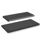
Datasheet Review and Symbol Validation
Thought for 3 mins 24 sec
Review result for W9825G6KH-6I
2) Datasheet metadata summary
Core device metadata
Special features
3) Absolute maximum ratings
4) Recommended operating conditions and electrical characteristics
Recommended operating conditions
DC characteristics
Capacitance
5) Pin descriptions from datasheet
Power, ground, and control pins
Address/data pins
6) Package dimensions
7) Cross-check of symbol and footprint vs datasheet
Critical findings
Confirmed symbol mismatches
Pins that do appear consistent
Bottom line
Step 2 was not needed: this part project already has a datasheet URL set in its properties, so no property update was required.
I was able to extract the datasheet content from mirrored copies of the same Winbond family datasheet: PDF and HTML. The existing Winbond URL in the part properties appears to serve a binary resource that was not directly readable by the file reader.
1) Available part information in this project
Table
| Field | Value |
|---|---|
| MPN | W9825G6KH-6I |
| Manufacturer | Winbond |
| Part type | Integrated Circuits |
| Description | 256 Mb SDRAM, 166 MHz, TSOP II 54 |
| Package from datasheet | TSOP II, 54-pin, 400 mil, 0.80 mm pitch |
| Schematic implementation | 54 individual terminal pins |
| PCB footprint presence | Yes, 54 pads present |
| Nets defined | None |
Table
| Parameter | Datasheet value |
|---|---|
| Memory organization | 4,194,304 words x 4 banks x 16 bits |
| Density | 256 Mb |
| Interface | LVTTL |
| Supply voltage | 3.3 V ± 0.3 V |
| Speed grade for -6I | 166 MHz / CL3 or 133 MHz / CL2 |
| Temperature grade for -6I | -40 °C to 85 °C |
| Package | TSOP II 54-pin, 400 mil, 0.80 mm pitch |
Table
| Feature | Datasheet value |
|---|---|
| CAS latency | 2, 3 |
| Burst lengths | 1, 2, 4, 8, full page |
| Refresh | 8K cycles / 64 ms at -40 °C to 85 °C |
| Self-refresh | Supported |
| Note | Self refresh not supported for TA > 85 °C |
| DQM | LDQM, UDQM byte masking |
| Precharge | Auto-precharge and controlled precharge |
| Power modes | Power-down, self-refresh |
Table
| Parameter | Rating |
|---|---|
| Any pin relative to VSS | -1 V to VDD + 0.5 V, limited to 4.6 V max |
| VDD/VDDQ relative to VSS | -1 V to 4.6 V |
| Operating temperature for -6I | -40 °C to 85 °C |
| Storage temperature | -55 °C to 150 °C |
| Soldering temperature | 260 °C for 10 s |
| Power dissipation | 1 W |
| Short-circuit output current | 50 mA |
Table
| Parameter | Min | Typ | Max |
|---|---|---|---|
| VDD | 3.0 V | 3.3 V | 3.6 V |
| VDDQ | 3.0 V | 3.3 V | 3.6 V |
| VIH | 2.0 V | - | VDD + 0.3 V |
| VIL | -0.3 V | - | 0.8 V |
| Operating temperature for -6I | -40 °C | - | 85 °C |
Table
| Parameter | Datasheet value |
|---|---|
| VOH | 2.4 V min at IOH = -2 mA |
| VOL | 0.4 V max at IOL = 2 mA |
| Input leakage | -5 µA to 5 µA |
| Output leakage | -5 µA to 5 µA |
| IDD1 operating current for -6I | 60 mA max |
| IDD2 standby current for -6I | 25 mA max |
| IDD2P power-down standby for -6I | 2 mA max |
| IDD3 no operating current for -6I | 35 mA max |
| IDD4 burst operating current for -6I | 80 mA max |
| IDD5 auto-refresh current for -6I | 75 mA max |
| IDD6 self-refresh current for -6I | 2 mA max |
Table
| Parameter | Max |
|---|---|
| CI | 3.8 pF |
| CCLK | 3.5 pF |
| CIO | 6.5 pF |
Table
| Pin/function | Datasheet description |
|---|---|
| VDD | Power for input buffers and logic circuit inside DRAM |
| VSS | Ground for input buffers and logic circuit inside DRAM |
| VDDQ | Power for I/O buffer, separated from VDD to improve DQ noise immunity |
| VSSQ | Ground for I/O buffer, separated from VSS to improve DQ noise immunity |
| CLK | System clock used to sample inputs on the rising edge |
| CKE | Controls clock activation/deactivation and entry to power-down, suspend, or self-refresh |
| CS | Chip select, enables/disables command decoder |
| RAS | Row address strobe command input |
| CAS | Column address strobe command input |
| WE | Write enable command input |
| LDQM / UDQM | Input/output mask pins for byte masking |
| NC | No connection |
Table
| Pin/function | Datasheet description |
|---|---|
| A0-A12 | Multiplexed row/column address inputs |
| A10/AP | Also selects auto-precharge behavior during precharge/read/write commands |
| BS0 / BS1 | Bank select inputs |
| DQ0-DQ15 | Multiplexed data input/output pins |
Table
| Dimension | Min | Nom | Max |
|---|---|---|---|
| D | 22.09 mm | 22.22 mm | 22.35 mm |
| E | 11.56 mm | 11.76 mm | 11.96 mm |
| E1 | 10.03 mm | 10.16 mm | 10.29 mm |
| Pitch e | - | 0.80 mm | - |
| Body height A | - | 0.95 mm | 1.05 mm |
| Lead length L | 0.40 mm | 0.50 mm | 0.60 mm |
Table
| Severity | Finding | Why it matters |
|---|---|---|
| Critical | The left-side symbol pin mapping is incorrect from pin 3 onward through pin 27. | This can cause a board wired to the wrong SDRAM pins, leading to total functional failure. |
| Critical | Several power and I/O supply pins are assigned to the wrong pin numbers. | This can cause incorrect power connection and possible device damage. |
| Critical | Several control/address pins are shifted to wrong numbers. | This will break memory initialization and bus operation even if the board is assembled correctly. |
| Medium | Footprint count appears correct at 54 pads, but geometric land pattern details were not exposed by the PCB inspector. | Pin count is consistent, but full mechanical verification of pad geometry/pitch in-project could not be completed from the available layout metadata. |
Table
| Project symbol pin | Project pin number | Datasheet expected at that pin number | Result |
|---|---|---|---|
| VDDQ_1 | 3 | DQ1 | Mismatch |
| DQ1 | 4 | DQ2 | Mismatch |
| DQ2 | 5 | VSSQ | Mismatch |
| VSSQ_1 | 6 | DQ3 | Mismatch |
| DQ4 | 8 | VDDQ | Mismatch |
| VDDQ_2 | 9 | DQ5 | Mismatch |
| VDD_2 | 14 | LDQM | Mismatch |
| LDQM | 15 | BS0 | Mismatch |
| ~WE | 16 | BS1 | Mismatch |
| ~CAS | 17 | A10/AP | Mismatch |
| ~RAS | 18 | A0 | Mismatch |
| ~CS | 19 | A1 | Mismatch |
| BS0 | 20 | A2 | Mismatch |
| BS1 | 21 | A3 | Mismatch |
| A10/AP | 22 | VDD | Mismatch |
| A0 | 23 | CS | Mismatch |
| A1 | 24 | RAS | Mismatch |
| A2 | 25 | CAS | Mismatch |
| A3 | 26 | WE | Mismatch |
| VDD_3 | 27 | VDDQ | Mismatch |
Table
Table
| Area | Verdict |
|---|---|
| Datasheet availability | Present |
| Part metadata completeness | Good after datasheet extraction |
| Symbol correctness | Fail - critical pin mapping errors |
| Footprint existence | Present |
| Footprint mechanical verification | Partial only |
| Risk if used as-is | High risk of nonfunctional or damaged hardware |
The most important issue is the symbol pin map from pins 3-27. That should be corrected before this part is used in any design.
@review check symbol issues
Inspect footprint geometry
Fetch exact pin map
To get started, talk to Flux or create a New Document.