Pin Function Grouping
Looking at the datasheet of this component, can you group together pins by their functions? for example for Power, 3v3, gnd_1 gnd_2 etc
NOTE: If you group them, can you not add the same pin if you already added them in a group? You should know which pin function is common for its function
Worked for 3 mins 21 sec
I grouped the USB4520 pins by function with no duplicate pin assignments: VBUS, Ground, Shield/Shell, USB2 Data, CC, SBU, and Dummy/NC. Full grouping is in the USB4520-03-0-A Pin Functional Groups project file.
Organize symbol pins
Check current symbol
Compare datasheet groups
Add signal names
Refine this doc
Ask about this doc
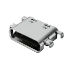
USB4520-03-0-A Pin Functional Groups
Source: GCT USB4520-03-0-A datasheet / product drawing pin assignment.
Grouping rule used: each physical contact is assigned to exactly one function group. Shared signals such as GND and VBUS are grouped by electrical function, but the same pin/contact is not repeated in any other group.
Recommended Functional Groups
Table
| Function group | Pins / contacts | Signal names | Suggested Flux Section | Suggested Pin Group | Notes |
|---|---|---|---|---|---|
| Power / VBUS | A4, A9, B4, B9 | VBUS | Power | VBUS | USB bus power contacts. These are duplicated for Type-C plug orientation and current sharing. |
| Ground | A1, A12, B1, B12 | GND | Ground | GND | Main return contacts. Keep only in Ground, not also in Shield. |
| Shield / Shell Ground | SHELL | SHELL / Shield / GND | Ground | Shield | Connector shell is tied to ground/shield function. Keep separate from signal GND contacts so the mechanical shell terminal is not duplicated. |
| USB 2.0 Data | A6, A7, B6, B7 | A6 = Dp1 / D+, A7 = Dn1 / D-, B6 = Dp2 / D+, B7 = Dn2 / D- | Communication | USB2 | A6 and B6 are the D+ pair duplicates; A7 and B7 are the D− pair duplicates. They are grouped together as USB2, not repeated in separate D+ / D− groups. |
| Configuration Channel | A5, B5 | CC1, CC2 | Communication | CC | USB Type-C configuration-channel pins. |
| Sideband Use | A8, B8 | SBU1, SBU2 | Communication | SBU | SBU pins are present on Type-C even though many USB 2.0-only designs leave them unconnected unless accessory/alternate-mode behavior is needed. |
| Dummy / No Connect SuperSpeed Positions | A2, A3, A10, A11, B2, B3, B10, B11 | Dummy / omitted SS contacts | No Connect | Dummy | These are the eight dummy positions in the “16 + 8 dummy” USB 2.0 Type-C receptacle. Do not duplicate them under USB2 data. |
Per-Contact Assignment Checklist
Table
| Contact | Assigned group | Signal |
|---|---|---|
| A1 | Ground | GND |
| A2 | Dummy / No Connect SuperSpeed Positions | Dummy / NC |
| A3 | Dummy / No Connect SuperSpeed Positions | Dummy / NC |
| A4 | Power / VBUS | VBUS |
| A5 | Configuration Channel | CC1 |
| A6 | USB 2.0 Data | Dp1 / D+ |
| A7 | USB 2.0 Data | Dn1 / D− |
| A8 | Sideband Use | SBU1 |
| A9 | Power / VBUS | VBUS |
| A10 | Dummy / No Connect SuperSpeed Positions | Dummy / NC |
| A11 | Dummy / No Connect SuperSpeed Positions | Dummy / NC |
| A12 | Ground | GND |
| B1 | Ground | GND |
| B2 | Dummy / No Connect SuperSpeed Positions | Dummy / NC |
| B3 | Dummy / No Connect SuperSpeed Positions | Dummy / NC |
| B4 | Power / VBUS | VBUS |
| B5 | Configuration Channel | CC2 |
| B6 | USB 2.0 Data | Dp2 / D+ |
| B7 | USB 2.0 Data | Dn2 / D− |
| B8 | Sideband Use | SBU2 |
| B9 | Power / VBUS | VBUS |
| B10 | Dummy / No Connect SuperSpeed Positions | Dummy / NC |
| B11 | Dummy / No Connect SuperSpeed Positions | Dummy / NC |
| B12 | Ground | GND |
| SHELL | Shield / Shell Ground | Shield / GND |
Notes
- If you want the schematic symbol to be compact, make one sub-symbol called Power containing VBUS, GND, and SHELL, and another called USB-C Signals containing USB2, CC, SBU, and Dummy/NC contacts.
- If you want strict functional separation, keep Shield / Shell Ground as its own group because it is a mechanical/shield connection, even though the drawing identifies it as GND.
- No contact is intentionally listed in more than one group above.


Welcome 👋
Flux accelerates your PCB design with AI.
Create your account to start using this component and bring your ideas to life.