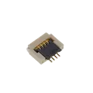
Part Specification Review
Thought for 5 mins 25 sec
Here’s a complete review and cross-check of your TF12S-4S-0.5SH(800) part project.
- Available part information found in the project
- Manufacturer: Hirose
- MPN: TF12S-4S-0.5SH(800)
- Description: FFC & FPC Connector (receptacle), 4 positions, 0.5 mm pitch, SMT right angle, bottom contact
- Designator Prefix: J
- Datasheet URL (already set): Datasheet
- Schematic symbol pins present: 1, 2, 3, 4, MP1, MP2
- Footprint pads present: 1, 2, 3, 4, MP1, MP2
- Datasheet URL check
- A datasheet URL is already present, so no change was made.
- Extracted specifications and metadata Primary sources:
- Official product page: https://www.hirose.com/product/p/CL0480-0319-0-00
- Specification Sheet (English): https://www.hirose.com/en/product/document?clcode=CL0480-0319-0-00&productname=TF12S-4S-0.5SH(800)&series=TF12&documenttype=SpecSheet&lang=en&documentid=D166078_en
- 2D Drawing (English): https://www.hirose.com/en/product/document?clcode=CL0480-0319-0-00&productname=TF12S-4S-0.5SH(800)&series=TF12&documenttype=2DDrawing&lang=en&documentid=D166077_en
TF12S-4S-0.5SH(800) — Extracted Specifications
| Category | Parameter | Value | Source |
| Mechanical | Mounting pitch | 0.5 mm | Product page |
| Mechanical | Connector length | 4.2 mm | Product page |
| Mechanical | Connector height | 1.0 mm | Product page |
| Mechanical | Connector width (depth) | 3.9 mm | Product page |
| Contacts | Positions | 4 | Product page |
| Contacts | Rows (cable/board) | 1 | Product page |
| Contacts | Contact pitch | 0.5 mm | Product page |
| Contacts | Contact orientation | Bottom | Product page |
| Insertion | FPC/FFC insertion direction | Horizontal | Product page |
| Actuator | Method | Back flip (Front Axis type) | Product page |
| Cable | Applicable FPC thickness | 0.2 mm | Product page |
| Electrical | Rated voltage (AC) | 50 V AC | Product page |
| Electrical | Rated voltage (DC) | 50 V DC | Product page |
| Electrical | Rated current | 0.5 A | Product page |
| Electrical | Contact resistance | 100 mΩ Max | Product page |
| Environmental | Operating temp (min) | -55 C | Product page |
| Environmental | Operating temp (max) | 85 C | Product page |
| Materials | Contact surface finish | Gold | Product page |
| Materials | Gold plating thickness | 0.05 µm | Product page |
| Durability | Mating cycles | 20 | Product page |
| Compliance | RoHS | Compliant | Product page |
| Packaging | Type | Reel | Product page |
| Packaging | Qty per reel | 5000 pcs | Product page |
| Packaging | Mass | 0.021 g | Product page |
| Packaging | Qty per box | 25000 pcs | Product page |
| Drawing | 2D drawing | Dimensions, land pattern, pin-1 mark | 2D Drawing (English) |
| Notes | Absolute Maximum Ratings | Not specified for this connector class; use ratings above | Product page |
Pin descriptions
- Functional pins: 4 signal contacts (positions 1–4) at 0.5 mm pitch; bottom contact; horizontal insertion; ZIF back-flip actuator.
- Mechanical pads: 2 metal hold-downs/tabs (commonly denoted MP1, MP2).
- Pin 1 orientation: Refer to the 2D Drawing (English) for the exact pin-1 marker and orientation. The product page does not display the mark inline.
- Cross-check: schematic symbol and footprint vs. datasheet What matches
- Pin count: Symbol shows four contacts 1, 2, 3, 4 which matches a 4-position receptacle.
- Mechanical pads: Symbol includes MP1 and MP2, consistent with typical metal hold-down tabs for this series.
- Designator prefix: Set to J, appropriate for connectors.
Items that require verification (potential risks)
- Land pattern geometry: The footprint pad sizes and spacing could not be auto-extracted from the 2D drawing. You should verify pad dimensions, solder mask/paste apertures, and courtyard against “2D Drawing – English” (D166077_en) to ensure manufacturability.
- Pitch confirmation on PCB: The layout API did not expose pad coordinates, so the 0.5 mm center-to-center pitch between contacts 1–4 could not be numerically verified here.
- Pin-1 mark and orientation: Confirm the Pin 1 location on the footprint silkscreen/pin numbering matches the drawing. Incorrect pin-1 orientation is a common cause of assembly issues.
- Keep-out and actuator clearance: Ensure the footprint provides adequate keep-out/clearance for the back-flip actuator mechanism per the drawing so the FPC can insert/remove freely.
- Board edge and component keep-outs: If the design plans to place this at a board edge for cable access, confirm the mechanical outline and insertion path align with the recommended dimensions in the 2D drawing.
If you want, I can verify the pad geometry and pin-1 location against the 2D drawing by measuring your footprint directly and list any specific mismatches to fix.
Check pad pitch precisely
Verify footprint vs 2D drawing
Confirm pin-1 marking
Add official Hirose link