Part Information Review and Update
Thought for 3 mins 25 sec
Part Review Summary
Key datasheet specs
Symbol and pin audit
Good
Important note on pin-map verification
I reviewed the current part project against the datasheet-driven part-sync checklist and checked the existing project metadata, schematic terminals, and footprint pads.
What I found
Metadata status
Table
| Item | Current project | Datasheet | Result |
|---|---|---|---|
| MPN | TC58NVG1S3HBAI6 | TC58NVG1S3HBAI6 | Match |
| Manufacturer | Toshiba | Toshiba | Match |
| Description | NAND Flash 3.3V 2Gb 24nm SLC NAND (EEPROM) | 3.3 V, 2 Gbit CMOS NAND E2PROM | Essentially match |
| Datasheet URL | Already present | Official Toshiba PDF located in project property | No web search/update needed |
| Part Type | Integrated Circuits | NAND flash memory | Acceptable but generic |
| Designator Prefix | IC | IC-style part | Acceptable |
| Package / case code | Not present | P-VFBGA67-0608-0.80-001 | Missing property |
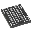
| Pin count | 67 terminals | 67-ball package | Match |
| Footprint pads | 67 pads | 67-ball package | Match by count |
Table
| Spec | Value |
|---|---|
| Device type | 3.3 V CMOS NAND flash memory |
| Density | 2 Gbit |
| Organization | 256M x 8 |
| Interface width | x8 |
| Page size | 2176 bytes total = 2048 + 128 |
| Block size | 128K + 8K bytes |
| Valid blocks | 2008 min, 2048 max |
| Supply voltage | 2.7 V to 3.6 V |
| Operating temperature | -40 C to 85 C |
| Read current | 30 mA max |
| Program current | 30 mA max |
| Erase current | 30 mA max |
| Standby current | 50 uA max |
| Access timing | 25 us array-to-register, 25 ns serial read cycle min |
| ECC note | 8-bit ECC per 512 bytes required |
- The project has 67 terminal components, which matches the 67-ball package requirement.
- The footprint also contains 67 pads, so the package ball count is consistent.
- The active signal names present in the symbol align with the datasheet signal set:
WP,ALE,VSS,CE,WE,RY/BY,RE,CLEI/O1toI/O8VCC
Table
| Area | Finding | Severity |
|---|---|---|
| Pin metadata | Every terminal I checked has Pin Type = Unspecified | High |
| Pin descriptions | No Pin Description properties are populated | High |
| Symbol organization | No Section, Pin Group, or Sub-symbol Designator Suffix properties are populated | Medium |
| Package metadata | Package or Case Code property is missing | Medium |
| Naming style | Project uses labels like VCC_1, VCC_2, VSS_1, VSS_2, VSS_3, which is workable, but the underlying semantic pin metadata is still missing | Medium |
| Footprint verification depth | I could confirm pad count, but not full mechanical ball pitch / land geometry from the current layout data alone | Medium |
The datasheet extraction for the BGA ball table is partially ambiguous in text form, but it clearly identifies the active balls and confirms this is a 67-ball package. Your project’s 67 terminals + 67 pads is the strongest structural sign that the footprint and symbol were built from the correct package basis. The larger problem is not ball count mismatch - it is that the pin semantics were never filled in. The audit criteria for exact pin-count matching and datasheet-as-source-of-truth come straight from the recommended workflow .
Bottom line
Overall assessment
- MPN / manufacturer / basic description: good
- Datasheet URL: already set, so no update was needed
- Package family and pin count: look consistent with the datasheet
- Main problem: the part is incomplete as a reusable library part because the terminals lack proper metadata
- Add
Package or Case Code = P-VFBGA67-0608-0.80-001 - Populate
Pin Typefor all 67 terminals - Add short
Pin Descriptionvalues - Assign
Section,Pin Group, andPin Orientation - Optionally refine the project description to include package and organization details
If you want, I can do the next step and sync the terminal properties to the datasheet so the symbol becomes fully annotated.
Fix flagged mismatches
Check missing datasheets
Audit package matches
Review one critical IC
To get started, talk to Flux or create a New Document.


Welcome 👋
Flux accelerates your PCB design with AI.
Create your account to start using this component and bring your ideas to life.