Pin Function Grouping
Thought for 1 sec
- Set PA8's Section to "GPIO"
- Set PA8's Pin Group to "PA"
- Set PA8's Pin Type to "Bi-Directional"
- Set PA8's Sub-symbol Designator Suffix to "GPIOA"
- Set PA9's Section to "GPIO"
- Set PA9's Pin Group to "PA"
- Set PA9's Pin Type to "Bi-Directional"
- Set PA9's Sub-symbol Designator Suffix to "GPIOA"
- Set PA10's Section to "GPIO"
- Set PA10's Pin Group to "PA"
- Set PA10's Pin Type to "Bi-Directional"
- Set PA10's Sub-symbol Designator Suffix to "GPIOA"
- Set PB2's Section to "GPIO"
- Set PB2's Pin Group to "PB"
- Set PB2's Pin Type to "Bi-Directional"
- Set PB2's Sub-symbol Designator Suffix to "GPIOB"
- Set PB5's Section to "GPIO"
- Set PB5's Pin Group to "PB"
- Set PB5's Pin Type to "Bi-Directional"
- Set PB5's Sub-symbol Designator Suffix to "GPIOB"
- Set PB6's Section to "GPIO"
- Set PB6's Pin Group to "PB"
- Set PB6's Pin Type to "Bi-Directional"
- Set PB6's Sub-symbol Designator Suffix to "GPIOB"
- Set PB7's Section to "GPIO"
- Set PB7's Pin Group to "PB"
- Set PB7's Pin Type to "Bi-Directional"
- Set PB7's Sub-symbol Designator Suffix to "GPIOB"
- Set PB8's Section to "GPIO"
- Set PB8's Pin Group to "PB"
- Set PB8's Pin Type to "Bi-Directional"
- Set PB8's Sub-symbol Designator Suffix to "GPIOB"
- Set PB9's Section to "GPIO"
- Set PB9's Pin Group to "PB"
- Set PB9's Pin Type to "Bi-Directional"
- Set PB9's Sub-symbol Designator Suffix to "GPIOB"
- Set PB10's Section to "GPIO"
- Set PB10's Pin Group to "PB"
- Set PB10's Pin Type to "Bi-Directional"
- Set PB10's Sub-symbol Designator Suffix to "GPIOB"
- Set PB11's Section to "GPIO"
- Set PB11's Pin Group to "PB"
- Set PB11's Pin Type to "Bi-Directional"
- Set PB11's Sub-symbol Designator Suffix to "GPIOB"
- Set PB12's Section to "GPIO"
- Set PB12's Pin Group to "PB"
- Set PB12's Pin Type to "Bi-Directional"
- Set PB12's Sub-symbol Designator Suffix to "GPIOB"
- Set PB13's Section to "GPIO"
- Set PB13's Pin Group to "PB"
- Set PB13's Pin Type to "Bi-Directional"
- Set PB13's Sub-symbol Designator Suffix to "GPIOB"
- Set PB14's Section to "GPIO"
- Set PB14's Pin Group to "PB"
- Set PB14's Pin Type to "Bi-Directional"
- Set PB14's Sub-symbol Designator Suffix to "GPIOB"
- Set PB15's Section to "GPIO"
- Set PB15's Pin Group to "PB"
- Set PB15's Pin Type to "Bi-Directional"
- Set PB15's Sub-symbol Designator Suffix to "GPIOB"
- Set PC6's Section to "GPIO"
- Set PC6's Pin Group to "PC"
- Set PC6's Pin Type to "Bi-Directional"
- Set PC6's Sub-symbol Designator Suffix to "GPIOC"
- Set PC7's Section to "GPIO"
- Set PC7's Pin Group to "PC"
- Set PC7's Pin Type to "Bi-Directional"
- Set PC7's Sub-symbol Designator Suffix to "GPIOC"
- Set PC8's Section to "GPIO"
- Set PC8's Pin Group to "PC"
- Set PC8's Pin Type to "Bi-Directional"
- Set PC8's Sub-symbol Designator Suffix to "GPIOC"
- Set PC9's Section to "GPIO"
- Set PC9's Pin Group to "PC"
- Set PC9's Pin Type to "Bi-Directional"
- Set PC9's Sub-symbol Designator Suffix to "GPIOC"
- Set PC10's Section to "GPIO"
- Set PC10's Pin Group to "PC"
- Set PC10's Pin Type to "Bi-Directional"
- Set PC10's Sub-symbol Designator Suffix to "GPIOC"
- Set PC11's Section to "GPIO"
- Set PC11's Pin Group to "PC"
- Set PC11's Pin Type to "Bi-Directional"
- Set PC11's Sub-symbol Designator Suffix to "GPIOC"
- Set PC12's Section to "GPIO"
- Set PC12's Pin Group to "PC"
- Set PC12's Pin Type to "Bi-Directional"
- Set PC12's Sub-symbol Designator Suffix to "GPIOC"
- Set PC13's Section to "GPIO"
- Set PC13's Pin Group to "PC"
- Set PC13's Pin Type to "Bi-Directional"
- Set PC13's Sub-symbol Designator Suffix to "GPIOC"
- Set PD0's Section to "GPIO"
- Set PD0's Pin Group to "PD"
- Set PD0's Pin Type to "Bi-Directional"
- Set PD0's Sub-symbol Designator Suffix to "GPIOD"
- Set PD1's Section to "GPIO"
- Set PD1's Pin Group to "PD"
- Set PD1's Pin Type to "Bi-Directional"
- Set PD1's Sub-symbol Designator Suffix to "GPIOD"
- Set PD2's Section to "GPIO"
- Set PD2's Pin Group to "PD"
- Set PD2's Pin Type to "Bi-Directional"
- Set PD2's Sub-symbol Designator Suffix to "GPIOD"
- Set PD3's Section to "GPIO"
- Set PD3's Pin Group to "PD"
- Set PD3's Pin Type to "Bi-Directional"
- Set PD3's Sub-symbol Designator Suffix to "GPIOD"
- Set PD4's Section to "GPIO"
- Set PD4's Pin Group to "PD"
- Set PD4's Pin Type to "Bi-Directional"
- Set PD4's Sub-symbol Designator Suffix to "GPIOD"
- Set PD5's Section to "GPIO"
- Set PD5's Pin Group to "PD"
- Set PD5's Pin Type to "Bi-Directional"
- Set PD5's Sub-symbol Designator Suffix to "GPIOD"
- Set PD6's Section to "GPIO"
- Set PD6's Pin Group to "PD"
- Set PD6's Pin Type to "Bi-Directional"
- Set PD6's Sub-symbol Designator Suffix to "GPIOD"
- Set PD7's Section to "GPIO"
- Set PD7's Pin Group to "PD"
- Set PD7's Pin Type to "Bi-Directional"
- Set PD7's Sub-symbol Designator Suffix to "GPIOD"
- Set PD8's Section to "GPIO"
- Set PD8's Pin Group to "PD"
- Set PD8's Pin Type to "Bi-Directional"
- Set PD8's Sub-symbol Designator Suffix to "GPIOD"
- Set PD9's Section to "GPIO"
- Set PD9's Pin Group to "PD"
- Set PD9's Pin Type to "Bi-Directional"
- Set PD9's Sub-symbol Designator Suffix to "GPIOD"
- Set PD10's Section to "GPIO"
- Set PD10's Pin Group to "PD"
- Set PD10's Pin Type to "Bi-Directional"
- Set PD10's Sub-symbol Designator Suffix to "GPIOD"
- Set PD11's Section to "GPIO"
- Set PD11's Pin Group to "PD"
- Set PD11's Pin Type to "Bi-Directional"
- Set PD11's Sub-symbol Designator Suffix to "GPIOD"
- Set PD12's Section to "GPIO"
- Set PD12's Pin Group to "PD"
- Set PD12's Pin Type to "Bi-Directional"
- Set PD12's Sub-symbol Designator Suffix to "GPIOD"
- Set PD13's Section to "GPIO"
- Set PD13's Pin Group to "PD"
- Set PD13's Pin Type to "Bi-Directional"
- Set PD13's Sub-symbol Designator Suffix to "GPIOD"
- Set PD14's Section to "GPIO"
- Set PD14's Pin Group to "PD"
- Set PD14's Pin Type to "Bi-Directional"
- Set PD14's Sub-symbol Designator Suffix to "GPIOD"
- Set PD15's Section to "GPIO"
- Set PD15's Pin Group to "PD"
- Set PD15's Pin Type to "Bi-Directional"
- Set PD15's Sub-symbol Designator Suffix to "GPIOD"
- Set PE0's Section to "GPIO"
- Set PE0's Pin Group to "PE"
- Set PE0's Pin Type to "Bi-Directional"
- Set PE0's Sub-symbol Designator Suffix to "GPIOE"
- Set PE1's Section to "GPIO"
- Set PE1's Pin Group to "PE"
- Set PE1's Pin Type to "Bi-Directional"
- Set PE1's Sub-symbol Designator Suffix to "GPIOE"
- Set PE2's Section to "GPIO"
- Set PE2's Pin Group to "PE"
- Set PE2's Pin Type to "Bi-Directional"
- Set PE2's Sub-symbol Designator Suffix to "GPIOE"
- Set PE3's Section to "GPIO"
- Set PE3's Pin Group to "PE"
- Set PE3's Pin Type to "Bi-Directional"
- Set PE3's Sub-symbol Designator Suffix to "GPIOE"
- Set PE4's Section to "GPIO"
- Set PE4's Pin Group to "PE"
- Set PE4's Pin Type to "Bi-Directional"
- Set PE4's Sub-symbol Designator Suffix to "GPIOE"
- Set PE5's Section to "GPIO"
- Set PE5's Pin Group to "PE"
- Set PE5's Pin Type to "Bi-Directional"
- Set PE5's Sub-symbol Designator Suffix to "GPIOE"
- Set PE6's Section to "GPIO"
- Set PE6's Pin Group to "PE"
- Set PE6's Pin Type to "Bi-Directional"
- Set PE6's Sub-symbol Designator Suffix to "GPIOE"
- Set PE7's Section to "GPIO"
- Set PE7's Pin Group to "PE"
- Set PE7's Pin Type to "Bi-Directional"
- Set PE7's Sub-symbol Designator Suffix to "GPIOE"
- Set PE8's Section to "GPIO"
- Set PE8's Pin Group to "PE"
- Set PE8's Pin Type to "Bi-Directional"
- Set PE8's Sub-symbol Designator Suffix to "GPIOE"
- Set PE9's Section to "GPIO"
- Set PE9's Pin Group to "PE"
- Set PE9's Pin Type to "Bi-Directional"
- Set PE9's Sub-symbol Designator Suffix to "GPIOE"
- Set PE10's Section to "GPIO"
- Set PE10's Pin Group to "PE"
- Set PE10's Pin Type to "Bi-Directional"
- Set PE10's Sub-symbol Designator Suffix to "GPIOE"
- Set PE11's Section to "GPIO"
- Set PE11's Pin Group to "PE"
- Set PE11's Pin Type to "Bi-Directional"
- Set PE11's Sub-symbol Designator Suffix to "GPIOE"
- Set PE12's Section to "GPIO"
- Set PE12's Pin Group to "PE"
- Set PE12's Pin Type to "Bi-Directional"
- Set PE12's Sub-symbol Designator Suffix to "GPIOE"
- Set PE13's Section to "GPIO"
- Set PE13's Pin Group to "PE"
- Set PE13's Pin Type to "Bi-Directional"
- Set PE13's Sub-symbol Designator Suffix to "GPIOE"
- Set PE14's Section to "GPIO"
- Set PE14's Pin Group to "PE"
- Set PE14's Pin Type to "Bi-Directional"
- Set PE14's Sub-symbol Designator Suffix to "GPIOE"
- Set PE15's Section to "GPIO"
- Set PE15's Pin Group to "PE"
- Set PE15's Pin Type to "Bi-Directional"
- Set PE15's Sub-symbol Designator Suffix to "GPIOE"
Thought
Thought
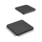
- Set Manufacturer Part Number to "STM32F407VGT6"
- Set Manufacturer Name to "STMicroelectronics"
- Set Package or Case Code to "100-LQFP"
- Set Designator Prefix to "U"
- Set Datasheet URL to "https://www.mouser.com/datasheet/2/389/stm32f405rg-1851084.pdf"
- Set Implementation Details to "Pin grouping updated from STM32F407VGT6 LQFP-100 pinout. Each of the 100 terminals has one Section and one Pin Group: Power/V..."
Thought for 2 sec
Updated all 100 STM32F407VGT6 terminals with a single functional Section, Pin Group, Pin Type, and sub-symbol grouping based on the LQFP-100 pinout: Power/Ground, Analog, Clock, Control, Debug, USB Communication, and GPIO-by-port. Verified the schematic still contains exactly 100 terminals and documented the grouping in STM32F407VGT6 Pin Grouping Summary.
Run ERC review
Find missing groups
Export grouping CSV
Recheck analog pins
Refine this doc
Ask about this doc
STM32F407VGT6 Pin Grouping Summary
Updated the STM32F407VGT6 LQFP-100 terminal properties so each pin belongs to exactly one functional Section and one Pin Group.
Grouping policy
- Power: VBAT, VDD pins, VDDA, VREF+, VCAP_1, VCAP_2
- Ground: VSS pins, VSSA
- Clock: PC14/PC15 as LSE, PH0/PH1 as HSE
- Control: NRST, BOOT0
- Communication: PA11/PA12 as USB
- Debug: PA13/PA14/PA15/PB3/PB4 as SWD/JTAG
- Analog: ADC-capable primary/common analog GPIOs PA0-PA7, PB0-PB1, PC0-PC5
- GPIO: remaining Port A/B/C/D/E pins grouped by port
Verification
- Total terminal count checked in the schematic: 100 terminals.
- Each terminal was assigned a single Section and a single Pin Group.
- Project metadata was updated for STM32F407VGT6, STMicroelectronics, 100-LQFP, and the datasheet URL.
Grouping policy
Verification