Part Review and Datasheet Analysis
Thought for 1 min 36 sec
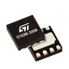
ST4SIM-300M part review
1) Available part information in the project
2) Datasheet status
Absolute maximum ratings
Recommended / operating conditions found
Pin descriptions from datasheet
VFDFPN8 package dimensions
Special features
4) Symbol and footprint cross-check
Major mismatches
Footprint geometry check
Conclusion
Recommended fixes
Table
| Field | Current project data | Review |
|---|---|---|
| MPN | ST4SIM-300M | Present |
| Manufacturer | STMicroelectronics | Present |
| Datasheet URL | Present: PDF | Already set, so no update was needed |
| Description | Project description is 123 | Incomplete / not usable |
| Package in footprint asset | SON127P600X500X100-9N.kicad_mod | Does not match datasheet naming cleanly |
| 3D model | ST4SIM-300M.stp | Present |
| Pin objects in symbol | 9 terminals | Includes an extra EP terminal |
| BOM metadata | Only generic GND entries are present | Part metadata is not fully populated in BOM |
A datasheet URL was already set on the part, so step 2 did not require a web search or property edit.
3) Datasheet summary
Device summary
Table
| Item | Datasheet value |
|---|---|
| Part | ST4SIM-300M |
| Function | GSMA eSIM / eUICC solution for IoT |
| Package options mentioned | VFDFPN8 5 × 6 mm wettable flank (MFF2), WLCSP24, card plugin 2FF / 3FF / 4FF |
| VFDFPN package pin count | 8 pins |
| Supply voltage | 1.8 V, 3 V |
| Operating temperature | -40 °C to +105 °C |
Table
| Symbol | Parameter | Value |
|---|---|---|
| VCC | Supply voltage | 1.8 to 3.0 V |
| VIO | Input/output voltage relative to ground | -0.3 to VCC + 0.3 V |
| TA | Ambient operating temperature | -40 to +105 °C |
| TSTG | Storage temperature | -65 to +150 °C |
| TLEAD | Lead temperature during soldering | See J-STD-020D note |
| VESD | HBM ESD | 4000 V |
Table
| Parameter | Value |
|---|---|
| Supply voltage | 1.8 V or 3 V |
| Operating temperature | -40 °C to +105 °C |
| Maximum VCC rising slope | 5 V/µs |
| Recommended VCC filtering | 100 nF and 1 µF on VCC |
Table
| Datasheet pin | Name | Function | Pin state |
|---|---|---|---|
| 1 | VCC | Power supply | - |
| 2 | RESET | External reset | Input pull-down |
| 3 | CLK | External clock | Pull-down |
| 4 | NC | Not connected internally | - |
| 5 | GND | Ground supply | - |
| 6 | SWIO | Not used | Input pull-up |
| 7 | I/O | Input/output | Pull-down then pull-up after card activation |
| 8 | NC | Not connected internally | - |
Table
| Parameter | Value |
|---|---|
| Overall size | 5.0 mm × 6.0 mm |
| Pitch | 1.27 mm |
Lead width b | 0.350 / 0.400 / 0.480 mm |
Lead length L | 0.400 / 0.500 / 0.600 mm |
Central bottom area D2 | 4.100 / 4.200 / 4.300 mm |
Central bottom area E2 | 3.300 / 3.400 / 3.500 mm |
Thickness A | 0.700 / 0.850 / 1.000 mm |
Table
| Area | Highlights |
|---|---|
| Connectivity | GSMA eSIM for IoT, remote SIM provisioning, up to 7 profiles optional |
| Network support | 2G / 3G / 4G LTE / CDMA / NB-IoT / CAT-M |
| Security | Common Criteria EAL6+, DES/3DES/AES, RSA up to 2048-bit, ECC up to 521-bit |
| Interfaces | ISO/IEC 7816-3 async I/O, SPI depending on package |
| Software ecosystem | Java Card v3.0.5 Classic, GlobalPlatform v2.3, GSMA SGP.32 v1.1 |
| Packaging | ECOPACK, MFF2 wettable-flank option |
Table
| Area | Project implementation | Datasheet | Risk |
|---|---|---|---|
| Pin numbering | Symbol/footprint map pin 1 = GND, 8 = VCC | Datasheet says pin 1 = VCC, 5 = GND | Critical: wrong PCB net assignment can cause immediate non-function or damage |
| Signal order | Project has 1 GND, 2 SWIO, 3 I/O, 4 NC, 5 NC, 6 CLK, 7 ~RESET, 8 VCC | Datasheet has 1 VCC, 2 RESET, 3 CLK, 4 NC, 5 GND, 6 SWIO, 7 I/O, 8 NC | Critical manufacturing failure risk |
| Extra pad/terminal | Project includes pin 9 / EP | Datasheet pin table defines 8 pins only | High: may create invalid net/pad definition and ordering confusion |
| Package naming | Footprint asset named SON127P600X500X100-9N | Datasheet calls package VFDFPN8 5 × 6 mm wettable flank (MFF2) | Medium: ordering/footprint selection ambiguity |
| Pin electrical types | All symbol terminals are Unspecified | Datasheet provides clear functional roles | Medium: weaker ERC quality, easier wiring mistakes |
Table
| Geometry item | Footprint | Datasheet | Review |
|---|---|---|---|
| Pin count | 8 edge pads + center pad = 9 pads | 8 pins | Mismatch |
| Edge pad pitch | 1.27 mm | 1.27 mm typ | Matches |
| Edge pad size | 0.45 × 0.95 mm | Lead width/length ranges support this as plausible land size | Looks reasonable |
| Body outline | 5 × 6 mm class | 5 × 6 mm | Matches broadly |
| Center pad size | 3.5 × 4.3 mm | Bottom central area 4.2 × 3.4 mm typ | Appears transposed relative to datasheet dimensions |
Table
| Severity | Finding |
|---|---|
| Critical | The current symbol-to-footprint pin numbering does not match the datasheet pinout. |
| Critical | If used as-is, this part could produce a board with incorrect power and signal routing. |
| High | The added EP / pin 9 is not supported by the datasheet pin table for the VFDFPN8 package. |
| Medium | The center pad dimensions appear swapped versus datasheet D2/E2. |
| Medium | Part metadata is incomplete, especially the description and pin-type definitions. |
Table
| Priority | Fix |
|---|---|
| 1 | Rebuild the symbol pin numbering to match datasheet VFDFPN8 exactly: 1 VCC, 2 RESET, 3 CLK, 4 NC, 5 GND, 6 SWIO, 7 I/O, 8 NC |
| 2 | Remove the extra EP electrical pin unless you confirm the package requires a center pad with a defined electrical function in the package drawing |
| 3 | Re-verify the center pad geometry against the VFDFPN8 mechanical drawing before release |
| 4 | Update the part description from 123 to a real functional description |
| 5 | Assign proper pin types so ERC can catch misuse |
If you want, I can next turn this into a clean correction checklist for the part project.
Create correction checklist
Inspect pin mapping
Recheck footprint geometry