Part Review and Datasheet Verification
Worked for 5 mins 30 sec
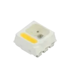
Completed the part review and created the detailed report: Part Review: SK6812MINIRGBW-NW-P6.
No critical pinout mismatch was found. The main flags are under-specified pin types/descriptions, a minor 3.5×3.7 vs 3.7×3.5 package-order wording difference, and footprint pad dimensions that could not be fully verified because the datasheet land-pattern drawing dimensions were not OCR-extracted.

Fix the pin types and add datasheet-based descriptions for all six terminals.
Thought for 5 sec
I’ll update the six terminal properties with datasheet-based pin types and descriptions, then re-read the symbol to verify the changes.
Worked for 22 sec
The descriptions are set; I’m normalizing the pin types to Flux’s standard values now.
Worked for 21 sec
Updated and verified all six terminal pin types and datasheet-based descriptions.
- NC: Not Connected
- GND: Ground
- DIN: Input
- VDD pins: Power In
- DOUT: Output
All descriptions now reflect the OPSCO datasheet functions.
Fix, verify, document
Update review doc
Run ERC/DRC
Verify footprint pads
Set public datasheet
Refine this doc
Ask about this doc
Part Review: SK6812MINIRGBW-NW-P6
Reviewed project metadata
- Project / part name:
SK6812MINIRGBW-NW-P6 - Manufacturer: Dongguan OPSCO Optoelectronics Co., Ltd.
- Manufacturer part number:
SK6812MINIRGBW-NW-P6 - Description: SMD 3.5 x 3.7 mm RGB LEDs with built-in IC, RoHS
- Mount: Surface Mount
- Part type: Integrated Circuits
- Pin count / pads: 6
- Existing Datasheet URL:
https://storage.googleapis.com/graviton-electric-symbols/document_assets/user-uploaded/086738ba747842befad3d004fcd7b87a4b3a9f98e7240c715dc37d18056897d2.pdf
The Datasheet URL was already populated, so I did not change it. A web search found the same OPSCO family datasheet as a public LCSC-hosted Rev. A/1 PDF for product code C7423107:
https://datasheet.lcsc.com/datasheet/pdf/a2bc892b0af22abe04f5c8a837afb921.pdf?productCode=C7423107. OPSCO’s own website lists the family download but does not expose a direct PDF link without its download flow.Datasheet source used
- Datasheet family P/N:
SK6812MINIRGBW-XX-P6-A-000 - Variant:
SK6812MINIRGBW-NW-P6-A-000 - Revision/date from OCR: Rev. A/1, 2025-07-22
- Manufacturer: Dongguan OPSCO Optoelectronic Technology Co., Ltd.
Key datasheet specifications
- Package: MINI 6-pin RGBW built-in IC LED, nominal 3.7 x 3.5 x 1.9 mm
- NW white CCT: 3800–4200 K
- White CRI note: Ra > 80 ±2
- Operating voltage: 3.7–5.5 V
- Operating temperature: -40 to +80 °C
- Storage temperature: -40 to +80 °C
- ESD withstand, HBM: 2 kV
- Data rate: 800 kbps typical
- PWM frequency: 4 kHz typical
- Static current: 0.29 mA typical at VDD = 5 V, outputs off
- Drive current: R/G/B 8 mA typical each; W 16.5 mA typical
- Wavelength / brightness:
- Red: 615–625 nm, 200–385 mcd
- Green: 525–535 nm, 580–1050 mcd
- Blue: 465–475 nm, 140–280 mcd
- NW white: 3800–4200 K, 1800–2525 mcd
- Logic thresholds: VIH min 0.65 × VDD; VIL max 0.35 × VDD
- Timing:
- Symbol period: min 1.20 µs
- T0H: 0.25–0.40 µs, typical 0.30 µs
- T0L: min 0.80 µs
- T1H: 0.65–1.00 µs, typical 0.75 µs
- T1L: min 0.20 µs
- Reset low: >200 µs
- Data format: 32-bit, high bit first, color order GRBW
- Application note: series protection resistors on DIN/DOUT recommended, about 500 Ω for short strip/hard-strip use; decoupling capacitors between LEDs are essential.
Pinout cross-check
Table
| Pin | Datasheet function | Project terminal | Result |
|---|---|---|---|
| 1 | NC, must not be used for circuit design | NC, Pin Number 1 | Match |
| 2 | GND, power ground | GND, Pin Number 2 | Match |
| 3 | DIN, control data input | DIN, Pin Number 3 | Match |
| 4 | VDD, power supply | VDD_1, Pin Number 4 | Match; name differs only to distinguish duplicate VDD terminal |
| 5 | DOUT, control data output | DOUT, Pin Number 5 | Match |
| 6 | VDD, power supply | VDD_2, Pin Number 6 | Match; name differs only to distinguish duplicate VDD terminal |
Symbol review
The schematic symbol exposes six terminals and the pin numbers/functions match the datasheet. The left/right symbol arrangement is also reasonable: NC/GND/DIN on the left, DOUT/VDD pins on the right. No pin-number mismatches were found.
Potential improvements:
- The project terminal
Pin Typeproperties are allUnspecified; these could be refined to NC/passive or power/data input/output semantics if desired. - Pin descriptions are not populated as explicit
Pin Descriptionproperties. The designator names carry the function, but adding descriptions from the datasheet would improve library quality. NCshould be documented as “do not connect / cannot be used for circuit design,” not merely no-connect.
Footprint review
The footprint contains six top-layer rectangular pads with designators matching the six datasheet pins. Layout data reports the following computed pad positions and sizes:
Table
| Pad | Position | Size | Shape/layer |
|---|---|---|---|
| NC | x=-0.0017, y=+0.0011 | 0.00065 x 0.0014 | rectangle, Top |
| GND | x=-0.0017, y=0 | 0.00065 x 0.0014 | rectangle, Top |
| DIN | x=-0.0017, y=-0.0011 | 0.00065 x 0.0014 | rectangle, Top |
| VDD_2 | x=+0.0017, y=+0.0011 | 0.00065 x 0.0014 | rectangle, Top |
| DOUT | x=+0.0017, y=0 | 0.00065 x 0.0014 | rectangle, Top |
| VDD_1 | x=+0.0017, y=-0.0011 | 0.00065 x 0.0014 | rectangle, Top |
Flux reports these values with unit
mm, but the numeric magnitudes appear internally scaled; interpreted as meters converted to mm, they correspond to a plausible ±1.7 mm x ±1.1 mm 6-pad footprint with ~0.65 x 1.4 mm pads. The datasheet OCR did not extract the numerical land-pattern dimensions from the drawing, so I could not independently verify each pad dimension from text. The footprint topology and pin order appear consistent with the datasheet top-view pinout.Mismatches / flags
No critical pinout mismatch was found.
Flags and recommended cleanups:
- Datasheet URL is already set to a user-uploaded copy. This is acceptable, but if you prefer a public distributor URL, use the LCSC Rev. A/1 PDF URL above.
- Pin descriptions and pin types are under-specified in the Flux part; add explicit
Pin Descriptionand more specificPin Typevalues for library clarity. - The package/property metadata says description 3.5 x 3.7 mm, while the datasheet text states MINI package size 3.7 x 3.5 x 1.9 mm. This is likely just width/length ordering, not an electrical mismatch.
- Footprint pad dimensions could not be fully checked because the datasheet land-pattern drawing dimensions were not OCR-extracted; visually/topologically the six-pad arrangement matches.
Reviewed project metadata
Datasheet source used
Key datasheet specifications
Pinout cross-check
Symbol review
Footprint review
Mismatches / flags