JST XH Connector Design Overview
3:18
Clarifying component design.
Understanding component linking.
Navigating linking rules.
Considering linking options.
Structuring project components and linking.
Accessing knowledge base.
Analyzing the schematic.
Reviewing the bill of materials.
Looking for "series pitch" in eXH.pdf
Looking for "rated current" in eXH.pdf
Looking for "rated voltage" in eXH.pdf
Looking for "operating temperature range" in eXH.pdf
Looking for "applicable wire" in eXH.pdf
Looking for "mating housing 3 circuits" in eXH.pdf
Looking for "S3B-XH-A footprint recommended pc board hole" in eXH.pdf
Looking for "right-angle header board edge" in eXH.pdf
Looking for "pin 1 mark" in eXH.pdf
Exploring alternative suggestions.
- Symbol pins: The schematic contains three passive terminals representing connector circuits:
- Interaction: As a connector library part, it has no nets inside this project. In a host design, these pins are wired to the target signals or rails. The PCB footprint provides plated through-holes (and boss hole if applicable) to mechanically and electrically anchor the connector.
Table
| Parameter | Value |
|---|---|
| Series pitch | 2.5 ±0.05 mm (series-defined; PCB layout shows 2.5 mm spacing) |
| Current rating | 3 A AC/DC (AWG #22) |
| Voltage rating | 250 V AC/DC |
| Operating temperature | -25 C to +85 C (including temperature rise under load) |
| Applicable wire | AWG #30 to AWG #22; insulation O.D. 0.9 mm to 1.9 mm |
| Mating housing (3 circuits) | XHP-3 |
| PCB hole sizes (reference) | Pins: φ0.9 +0.1/0 mm; Boss: φ1.7 +0.1/0 mm |
| PCB hole pitch tolerance | ±0.05 mm; shall not accumulate (per note) |
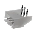
- Schematic symbol: Three passive terminals (1, 2, 3) expose the connector circuits. Pin numbering follows the datasheet convention (datasheet references “No. 1 circuit”).
- Footprint intent: Through-hole pads at 2.5 mm pitch sized per datasheet, plus a boss hole when required by the specific header variant. The right-angle, side-entry form factor implies a board-edge setback (“dimension C” in the datasheet) to ensure the shroud clears the PCB edge.
- Mechanical alignment: The boss hole and keepouts provide anti-rotation and insertion guidance; pad sizes and tolerances follow JST’s notes (e.g., hole pitch tolerance ±0.05 mm and non-accumulating).
- Right-angle THT vs vertical or SMT:
- Pros: Excellent mechanical robustness, convenient side-entry cable, suited for hand or wave soldering.
- Cons: Larger board-edge footprint, assembly height over board edge, not ideal for tight enclosures.
- 2.5 mm pitch vs denser families: Good balance for up to 3 A per datasheet with AWG #22; larger than 2.0 mm families (e.g., PH) but easier to hand-assemble and more forgiving mechanically.
- Hole sizing and tolerances: Using datasheet drill sizes and tolerance guidance improves fit across board vendors and drilling methods; consider slightly larger pin holes on hard FR-4 as JST advises.
- Board-edge clearance: Observe JST’s “dimension C” for side-entry headers to avoid mechanical clash with the shroud and latch features.
- Soldering process: Through-hole parts favor wave or selective solder; ensure thermal reliefs and solder-side clearances. Avoid copper pours too close to holes to prevent wicking.
- Current and temperature: Respect the 3 A rating (AWG #22). In high-ambient or limited airflow, derate current to maintain temperature rise within the -25 C to +85 C operating range.
- Tolerance stack-up: Hole pitch tolerance is ±0.05 mm and must not accumulate; keep global datum references consistent to prevent fit issues.
- Strain relief: Cables can exert side loads on right-angle headers; consider housing latch orientation and enclosure features to mitigate stress.
- Low-voltage power input (5–24 V) and distribution up to 3 A per circuit.
- Simple sensor or peripheral harnesses where keyed, shrouded connections are preferred.
- Field-serviceable modules that benefit from robust, widely available crimp housings like XHP-3.
- Symbol and footprint clarity:
- Add an explicit Pin 1 marker on silkscreen and assembly layers aligned with the datasheet “No. 1 circuit”.
- Include a clear courtyard per IPC guidance to aid DFM checks.
- Mechanical fidelity:
- Ensure the boss hole is present and correctly located for the specific S3B-XH-A variant; add keepout behind the connector to reflect housing overhang.
- Document and implement the board edge setback (“dimension C”) per the datasheet’s side-entry guidance.
- Metadata and usability:
- Add distributor links and full MPN metadata to streamline sourcing.
- Provide a 3D model and correct height to improve enclosure checks.
- Variants and scalability:
- Offer alternate footprints for top-entry or SMT headers as separate parts to cover more mechanical scenarios and assembly flows.
- Provide housing and crimp contact references in documentation so users can choose complete mating sets based on wire gauge and insulation O.D.
- The schematic’s pin objects (1, 2, 3) are passive and un-netted here by design; connectivity is defined in the end design where the connector is used.
- The project properties indicate “Max Current: 3A”; this matches the datasheet’s “Current rating: 3 A AC/DC (AWG #22)”. Always confirm against cable gauge and thermal environment.
Ready.
To get started, talk to Flux or create a New Document.
Reviews
Documents
Documents are markdown text files which describe project goals, capture details, or even simulation outputs.
Assets
S3B-XH-A_LF__SN_.step
3D3D Model
S3B-XH-A(LF)(SN).png
S3B-XH-A(LF)(SN)Thumbnail
S3B-XH-A(LF)(SN)
defaultDefaultJST_S3B-XH-A(LF)(SN).kicad_mod
FOOTPRINT_V5FootprintS3B-XH-A(LF)(SN)
Properties
Connector
JST Sales America Inc.
S3B-XH-A(LF)(SN)
P
Pricing & Availability
Distributor | Qty 1 |
|---|
Controls
Welcome 👋
Flux accelerates your PCB design with AI.
Create your account to start using this component and bring your ideas to life.