Project Overview: JST PH Connector
3:30
Clarifying component specs.
Gathering BOM and knowledge.
Exploring layout and linking components.
Linking components and referencing datasheets.
Accessing knowledge base.
Reviewing the bill of materials.
Analyzing the schematic.
Analyzing the PCB layout.
Looking for "PH series overview and features" in ePH.pdf
Looking for "pitch value" in ePH.pdf
Looking for "number of circuits positions 3" in ePH.pdf
Looking for "right angle surface mount type SM4-TB" in ePH.pdf
Looking for "current rating" in ePH.pdf
Looking for "voltage rating" in ePH.pdf
Looking for "operating temperature range" in ePH.pdf
Looking for "mating housing and contacts" in ePH.pdf
Looking for "recommended PCB land pattern" in ePH.pdf
Looking for "pin numbering and keying" in ePH.pdf
Looking for "board mounting style TB top entry or side entry" in ePH.pdf
Looking for "mechanical retention tabs strength" in ePH.pdf
Extracting datasheet information.
Creating the Project Overview.
- A library part for the 3‑pin, 2.0 mm‑pitch JST PH series, right‑angle, surface‑mount header: S3B-PH-SM4-TB(LF)(SN). It provides the schematic symbol and PCB footprint so you can place and wire this connector in your designs.
- Provide a reliable, compact wire‑to‑board interface for low‑power I/O or power leads where a 2.0 mm pitch, low profile, side‑entry (right‑angle) SMT header is desired.
- Standardize symbol/footprint mapping so downstream schematics, layout, DRC, and manufacturing exports are consistent.
- Schematic symbol: three passive terminals — Pin_1, Pin_2, Pin_3. These represent the three circuits/pins of the connector and will be connected to your nets in the schematic.
- PCB footprint: three SMT pads named to match pins 1–3. The symbol pins map 1:1 to footprint pads (Pad 1->Pin_1, etc.), ensuring the netlist drives correct copper pad connectivity at layout.
- Series: JST PH (wire‑to‑board, crimp style), 2.0 mm pitch, surface‑mount headers.
- Header family and model coverage includes S3B‑PH‑SM4‑TB, with 2–16 positions available in the series.
- From the JST PH series datasheet Datasheet:
- Pitch: 2.0 mm
- Current rating: 2 A AC/DC (AWG 24)
- Voltage rating: 100 V AC/DC
- Operating temperature: -40 C to +105 C (including temperature rise)
- Mating housings: e.g., PHR-3 (for 3 circuits)
- Crimp contacts: SPH-002T-P0.5S, SPH-002T-P0.5L (low‑insertion‑force option)
- SMT land pattern guidance (tolerances such as 2 ± 0.05 mm pitch; pattern dimensions and edge clearance for side‑entry) with notes to observe pitch tolerance ± 0.05 and not accumulate.
- The datasheet indicates pin‑1 marking and shows “No. 1 circuit” callouts on both symbol/land drawings; the footprint/silkscreen should reflect this.
- Schematic
- PCB footprint
- Three SMT pads correspond to the connector terminals; side‑entry geometry assumes the part sits at a board edge with specified keep‑back per datasheet notes (e.g., “Side edge of header on PCB” callout).
- Pin‑1 marker should be present and consistent with the datasheet orientation.
- Paste aperture and mask openings should follow land pattern guidance for reliable solder fillets and to manage mechanical loads from cable insertion/removal.
- Right‑angle SMT versus through‑hole
- Pros: fast SMT assembly, low profile, minimal drill hits; good for compact designs.
- Cons: less robust to off‑axis cable forces vs through‑hole posts; pay special attention to pad anchoring and copper distribution.
- 2.0 mm PH versus smaller/larger families
- 2.0 mm offers a balance of compact size and current capability (2 A with AWG 24). Smaller pitch reduces size but typically lowers current and increases crimp fineness; larger pitch improves ruggedness but costs area.
- Pin‑1 marking and orientation
- Strictly align symbol pin numbering to the header’s molded pin‑1 mark and the datasheet’s “No. 1 circuit” callouts to avoid wiring reversals in the mating harness.
- Current and thermal headroom
- The datasheet rating is 2 A (AWG 24). Consider derating in warm environments or with continuous high current. If needed, parallel pins for return paths or move to a higher‑current family.
- Mechanical stress on SMT right‑angle headers
- Repeated cable cycling or side‑loads can peel pads. Use ample pad area, adequate paste volume, solder fillets, and copper tie‑ins to inner layers where feasible. Consider board stiffening near the edge.
- Board‑edge clearance and keep‑outs
- Honor the land pattern’s side‑edge and keep‑back dimensions to ensure the housing clears the board edge and reflow fillets form correctly.
- ESD and transient exposure
- Exposed connector pins can see ESD. Add line protection as appropriate (for example a TVS Diode) on sensitive lines.
- Mating hardware availability
- You will need the correct housing and crimp contacts (e.g., PHR-3 with SPH-002T-P0.5S or SPH-002T-P0.5L). Ensure your supply chain supports both the PCB header and the mating cable set.
- Low‑power battery leads, small peripheral power connectors, fan/sensor interfaces, or general three‑wire connections (V+, GND, signal) where compact size and serviceability are needed.
- Symbol consistency and metadata
- The schematic parts show a “P” designator prefix on the terminals; for connectors it’s typical to use “J”. Consider publishing the symbol as a single connector instance with designator prefix “J” and named pins “1–3”.
- Silkscreen and assembly layers
- Ensure a clear, unambiguous pin‑1 marker; add assembly and courtyard outlines with realistic assembly tolerances for pick‑and‑place.
- Land pattern refinements
- Validate pad sizes and edge clearances exactly against the datasheet SMT land pattern and its ± 0.05 mm pitch tolerance note; tune paste aperture reductions to balance solder volume and mechanical strength.
- 3D model alignment
- Include/verify a 3D model aligned to the footprint to catch mechanical interferences (especially at the board edge or with nearby tall parts).
- Variants and scalability
- Publish matching 2–16 position variants in the same family for consistent adoption across designs; add parametric fields (position count, pitch, right‑angle/vertical) to ease part selection.
- Schematic symbol exposes three terminals:
- Footprint provides three matching pads for the right‑angle SMT header.
- Datasheet‑backed specs include 2.0 mm pitch, 2 A (AWG 24), 100 V, -40 C to +105 C, and specific SMT land pattern guidance Datasheet.
Ready.
To get started, talk to Flux or create a New Document.
Reviews
Documents
Documents are markdown text files which describe project goals, capture details, or even simulation outputs.
Assets
JST_PH_S3B-PH-SM4-TB_1x03-1MP_P2.00mm_Horizontal.kicad_mod
FOOTPRINT_V5Footprint
Conn_01x03
defaultDefault
S3B-PH-SM4-TB(LF)(SN)-thumb.png
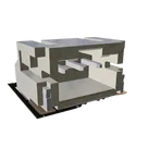
S3B-PH-SM4-TB(LF)(SN)-thumbThumbnailS3B-PH-SM4-TB(LF)(SN)--3DModel-STEP-56544.STEP
3D3D ModelS3B-PH-SM4-TB(LF)(SN)
Properties
Connector
JST Sales America Inc.
S3B-PH-SM4-TB(LF)(SN)
J
Pricing & Availability
Distributor | Qty 1 |
|---|
Controls
Welcome 👋
Flux accelerates your PCB design with AI.
Create your account to start using this component and bring your ideas to life.