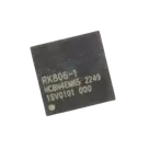
RK806-1 Pinout Verification
Worked for 3 mins 56 sec
Fixed the RK806-1 terminal Pin Type assignments from the datasheet.
Key changes:
VCCx,VCCA,VCC11–14→ Power InSWx,NLDOx,PLDOx,VCCIO→ Power OutVOUTx,FBx,PWRON,CS,CLK/SCL,VDC→ InputMOSI/SDA,MISO/PWRCRTL3,SYNC,SYNC_CLK,EXT_EN,RESETB,PWRCRTL1/2→ Bi-DirectionalINT→ OutputePAD→ Ground
I verified the updated properties and the part review checks show no unresolved terminal/property warnings or errors. Note: I only changed Pin Type as requested; the older Terminal Type metadata is still present but should no longer be the authoritative pin classification.

Search through all the pins of this part, see if there's invalid values like [Object Object]?
Thought for 17 sec
I’ll inspect every RK806-1 pin property directly from the schematic and look for malformed values such as
[Object Object] in pin names, pin numbers, pin types, descriptions, and related terminal metadata.Worked for 1 min 11 sec
I scanned all 69 RK806-1 terminals/pins.
No
[Object Object]-style malformed values were found in the visible pin properties. The structured Symbol Pin Position values are valid JSON/vector data, not malformed text.One thing to note: every terminal shows its internal
Pins: entry as undefined, but the actual terminal metadata is present and valid: designator, pin number, pin type, section, group, and symbol position. The terminal review checks also returned no unresolved pin/property issues.Fix undefined pins
Review SW9 properties
Check datasheet pins
Ignore-safe properties
Refine this doc
Ask about this doc
RK806-1 Pin Function Grouping
Source: Rockchip RK806 datasheet V1.4 pin description table. Each package pin is listed exactly once in the grouping below; duplicate-name package pins such as VCC1/VCC2/SW1/SW2 are listed by pin number so the physical pins remain distinct.
Ground / Thermal
- Exposed ePAD: Ground
Buck regulator input supplies
- Pin 1 VCC9: Power supply of buck9
- Pin 7 VCC8: Power supply of buck8
- Pin 22 VCC4: Power supply of buck4
- Pin 27 VCC10: Power supply of buck10
- Pin 28 VCC6: Power supply of buck6
- Pin 33 VCC2: Power supply of buck2
- Pin 34 VCC2: Power supply of buck2
- Pin 43 VCC7: Power supply of buck7
- Pin 44 VCC5: Power supply of buck5
- Pin 52 VCC1: Power supply of buck1
- Pin 53 VCC1: Power supply of buck1
- Pin 54 VCC3: Power supply of buck3
Buck switching nodes
- Pin 6 SW8: Switching node of buck8
- Pin 23 SW4: Switching node of buck4
- Pin 26 SW10: Switching node of buck10
- Pin 29 SW6: Switching node of buck6
- Pin 35 SW2: Switching node of buck2
- Pin 36 SW2: Switching node of buck2
- Pin 42 SW7: Switching node of buck7
- Pin 45 SW5: Switching node of buck5
- Pin 50 SW1: Switching node of buck1
- Pin 51 SW1: Switching node of buck1
- Pin 55 SW3: Switching node of buck3
- Pin 68 SW9: Switching node of buck9
Buck feedback / output sense pins
- Pin 5 VOUT8: Output feedback voltage of buck8
- Pin 24 VOUT4: Output feedback voltage of buck4
- Pin 25 VOUT10: Output feedback voltage of buck10
- Pin 30 VOUT6: Output feedback voltage of buck6
- Pin 31 FB6: Extended divided resistor mode feedback voltage of buck6
- Pin 37 VOUT2: Output feedback voltage of buck2
- Pin 38 FB2: External divided resistor mode feedback voltage of buck2
- Pin 41 VOUT7: Output feedback voltage of buck7
- Pin 46 VOUT5: Output feedback voltage of buck5
- Pin 47 FB5: External divided resistor mode feedback voltage of buck5
- Pin 48 FB1: External divided resistor mode feedback voltage of buck1
- Pin 49 VOUT1: Output feedback voltage of buck1
- Pin 56 VOUT3: Output feedback voltage of buck3
- Pin 66 FB9: External divided resistor mode feedback voltage of buck9
- Pin 67 VOUT9: Output feedback voltage of buck9
LDO output pins
- Pin 8 NLDO5: NMOS LDO5 output
- Pin 10 NLDO4: NMOS LDO4 output
- Pin 11 NLDO3: NMOS LDO3 output
- Pin 12 NLDO2: NMOS LDO2 output
- Pin 14 NLDO1: NMOS LDO1 output
- Pin 57 PLDO3: PMOS LDO3 output
- Pin 58 PLDO2: PMOS LDO2 output
- Pin 60 PLDO1: PMOS LDO1 output
- Pin 63 PLDO4: PMOS LDO4 output
- Pin 65 PLDO5: PMOS LDO5 output
LDO / analog / interface supplies
- Pin 9 VCC14: Power supply of NLDO4/5
- Pin 13 VCC13: Power supply of NLDO1/2/3
- Pin 20 VCCIO: Output for I2C/SPI
- Pin 21 VCCA: Analog power supply; supply of PLDO6/RESETB/INT and system logic
- Pin 59 VCC11: Power supply of PLDO1/2/3
- Pin 64 VCC12: Power supply of PLDO4/5
Communication interface pins
- Pin 15 MOSI/SDA: SPI MOSI / I2C SDA
- Pin 16 MISO/PWRCRTL3: SPI MISO / PWRCRTL3 control
- Pin 17 CLK/SCL: SPI CLK / I2C SCL
- Pin 18 CS: Select SPI/I2C mode at power-on; SPI chip-select in SPI mode
Control, reset, interrupt, and enable pins
- Pin 4 PWRON: Power-on key; internal pull-up about 45 kΩ to VCCA
- Pin 19 INT: Interrupt
- Pin 32 VDC: VDC power-on signal
- Pin 39 EXT_EN: Control extended DCDC enable; master/slave select
- Pin 40 RESETB: Reset AP; equivalent capacitance to GND must not exceed 0.3 µF
- Pin 61 PWRCRTL2: PWRCRTL2 control
- Pin 62 PWRCRTL1: PWRCRTL1 control
Synchronization / clock pins
- Pin 2 SYNC: Master/slave synchronization signal
- Pin 3 SYNC_CLK: 32 kHz synchronization clock
Ground / Thermal
Buck regulator input supplies
Buck switching nodes
Buck feedback / output sense pins
LDO output pins
LDO / analog / interface supplies
Communication interface pins
Control, reset, interrupt, and enable pins
Synchronization / clock pins