Move Footprint in PCB Layout

can you make this foot print to the right of the Connector?
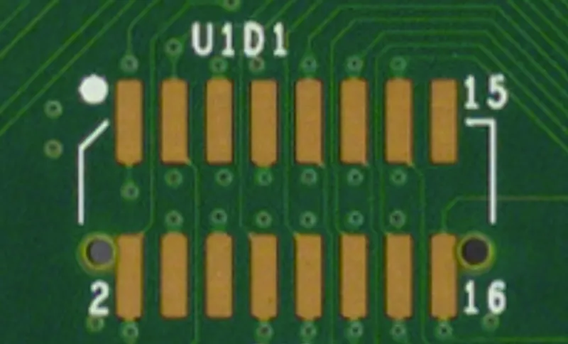
image_2026-04-24_180643536.png

Image

0:32

Thought for 5 sec

Yes, but not in this project - you only have view access here.
Your image looks like a 16-pin, dual-row footprint with a pin-1 marker, so the change you want is clear. I can help you do it in an editable copy instead.
If you want, I can also help you phrase the exact placement more precisely, like:
  • aligned horizontally
  • same vertical center
  • specific gap in mm
Set 2mm gap
Align centers
Use exact spacing

Finished working

To get started, talk to Flux or create a New Document.

Documents

    Documents are markdown text files which describe project goals, capture details, or even simulation outputs.

    Assets

    Conn_01x06

    Conn_01x06

    defaultDefault
    kicad_mod

    PinSocket_1x06_P2.54mm_Vertical.kicad_mod

    FOOTPRINT_V5Footprint
    1x06 V.png

    1x06 V.png

    1x06 VThumbnail
    step

    PinSocket_1x06_P2.54mm_Vertical.step

    3D3D Model

    Pin Socket 01x06 2.54mm Vertical

    Pin Socket 01x06 2.54mm Vertical thumbnail
    Through Hole straight socket strip, 01x06, 2.54mm pitch, single row #connector #pinsocket #tht

    Properties

    Connector

    J

    Pricing & Availability

    Distributor

    Qty 1

    Controls