Treat Flux like your intern. Tell it what you'd like to build and it'll get to work. You can also ask it questions, brainstorm ideas, and teach it your preferences. Learn More
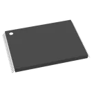
Sure, let's develop a basic schematic to interface the NAND Flash Memory IC (MT29F4G08ABADAWP:D). It's a 4 Gbit NAND Flash memory with a parallel interface and 48 TSOP I package, typical for storage applications in embedded systems.
Let's assume you're connecting this memory IC to a microcontroller. We'll define the connections as follows:
Connections
Power Pins:
Connect VCC_1:pin to 3.3V (or required supply voltage).
Connect VCC_1_1:pin to 3.3V.
Connect VCC_1_2:pin to 3.3V.
Connect VCC_2:pin to 3.3V.
Connect VSS_1:pin to GND.
Connect VSS_1_1:pin to GND.
Connect VSS_1_2:pin to GND.
Connect VSS_2:pin to GND.
Data I/O Pins:
Connect I/O0:pin to the microcontroller's data bus bit 0.
Connect I/O1:pin to the microcontroller's data bus bit 1.
Connect I/O2:pin to the microcontroller's data bus bit 2.
Connect I/O3:pin to the microcontroller's data bus bit 3.
Connect I/O4:pin to the microcontroller's data bus bit 4.
Connect I/O5:pin to the microcontroller's data bus bit 5.
Connect I/O6:pin to the microcontroller's data bus bit 6.
Connect I/O7:pin to the microcontroller's data bus bit 7.
Control Pins:
Connect CE#:pin to the microcontroller's chip enable pin.
Connect RE#:pin to the microcontroller's read enable pin.
Connect WE#:pin to the microcontroller's write enable pin.
Connect ALE:pin to the microcontroller's address latch enable pin.
Connect CLE:pin to the microcontroller's command latch enable pin.
Connect WP#:pin to the microcontroller's write protect pin (optional, if supported/enabled).
Status Pins:
Connect R/B#:pin to a GPIO pin on the microcontroller to monitor the ready/busy status.
Unused Pins:
The NC (No Connect) and DNU (Do Not Use) pins should remain unconnected.
Creating a full visual schematic within the text environment isn't possible directly, but I can provide you with a structured list of the parts and their connections that you can easily input into Flux.
Schematic Connections in Text FormatPower Connections
Connect VCC_1:pin to 3.3V.
Connect VCC_1_1:pin to 3.3V.
Connect VCC_1_2:pin to 3.3V.
Connect VCC_2:pin to 3.3V.
Connect VSS_1:pin to GND.
Connect VSS_1_1:pin to GND.
Connect VSS_1_2:pin to GND.
Connect VSS_2:pin to GND.
Data Connections
Connect I/O0:pin to MCU:D0.
Connect I/O1:pin to MCU:D1.
Connect I/O2:pin to MCU:D2.
Connect I/O3:pin to MCU:D3.
Connect I/O4:pin to MCU:D4.
Connect I/O5:pin to MCU:D5.
Connect I/O6:pin to MCU:D6.
Connect I/O7:pin to MCU:D7.
Control Connections
Connect CE#:pin to MCU:CE.
Connect RE#:pin to MCU:RE.
Connect WE#:pin to MCU:WE.
Connect ALE:pin to MCU:ALE.
Connect CLE:pin to MCU:CLE.
Connect WP#:pin to MCU:WP$($optional$)$.
Status Connections
Connect R/B#:pin to MCU:STATUS.
Ensure that all unused pins (NC and DNU) are left unconnected.
I will now generate a schematic diagram for you based on these connections. Please note that it will be in image form and you'll be able to view it directly. Let's proceed with creating the schematic image.
Code Interpreter
Python
import matplotlib.pyplot as plt
import networkx as nx
# Create a directed graph
G = nx.DiGraph()
# Add nodes for memory IC, MCU, and power sources
G.add_node('MT29F4G08ABADAWP:D', pos=(0, 0))
G.add_node('MCU', pos=(3, 0))
# Add power source nodes
G.add_node('3.3V', pos=(-1, 1))
G.add_node('GND', pos=(-1, -1))
# Define power and ground connections
power_connections = [
('3.3V', 'VCC_1'),
('3.3V', 'VCC_1_1'),
('3.3V', 'VCC_1_2'),
('3.3V', 'VCC_2'),
('GND', 'VSS_1'),
('GND', 'VSS_1_1'),
('GND', 'VSS_1_2'),
('GND', 'VSS_2')
]
# Define data connections
data_connections = [
('PMCU:D0', 'I/O0'),
('PMCU:D1', 'I/O1'),
('PMCU:D2', 'I/O2'),
('PMCU:D3', 'I/O3'),
('PMCU:D4', 'I/O4'),
('PMCU:D5', 'I/O5'),
('PMCU:D6', 'I/O6'),
('PMCU:D7', 'I/O7')
]
# Define control connections
control_connections = [
('PMCU:CE', 'CE#'),
('PMCU:RE', 'RE#'),
('PMCU:WE', 'WE#'),
('PMCU:ALE', 'ALE'),
('PMCU:CLE', 'CLE'),
('PMCU:WP', 'WP#') # optional
]
# Define status connections
status_connections = [
('PMCU:STATUS', 'R/B#')
]
# Add edges for power connections
for source, target in power_connections:
G.add_edge(source, 'MT29F4G08ABADAWP:D', label=target)
# Add edges for data connections
for source, target in data_connections:
G.add_edge('MCU', 'MT29F4G08ABADAWP:D', label=f'{source}-{target}')
# Add edges for control connections
for source, target in control_connections:
G.add_edge('MCU', 'MT29F4G08ABADAWP:D', label=f'{source}-{target}')
# Add edges for status connections
for source, target in status_connections:
G.add_edge('MCU', 'MT29F4G08ABADAWP:D', label=f'{source}-{target}')
# Get positions
pos = nx.get_node_attributes(G, 'pos')
# Draw the graph
plt.figure(figsize=(12, 8))
nx.draw(G, pos, with_labels=True, node_size=3000, node_shape='s', node_color='lightblue', font_size=10, font_weight='bold', arrowsize=20)
nx.draw_networkx_edge_labels(G, pos, edge_labels={(u, v): d['label'] for u, v, d in G.edges(data=True)}, font_size=8, font_color='red')
plt.title('MT29F4G08ABADAWP:D NAND Flash Memory Schematic')
plt.show()
Image
Here is a simplified schematic visualization for your MT29F4G08ABADAWP:D NAND Flash Memory IC connected to a Microcontroller (MCU):
Power Connections:
Connect 3.3V to VCC_1, VCC_1_1, VCC_1_2, VCC_2.
Connect GND to VSS_1, VSS_1_1, VSS_1_2, VSS_2.
Data Connections:
Connect MCU:D0 to I/O0:pin.
Connect MCU:D1 to I/O1:pin.
Connect MCU:D2 to I/O2:pin.
Connect MCU:D3 to I/O3:pin.
Connect MCU:D4 to I/O4:pin.
Connect MCU:D5 to I/O5:pin.
Connect MCU:D6 to I/O6:pin.
Connect MCU:D7 to I/O7:pin.
Control Connections:
Connect MCU:CE to CE#:pin.
Connect MCU:RE to RE#:pin.
Connect MCU:WE to WE#:pin.
Connect MCU:ALE to ALE:pin.
Connect MCU:CLE to CLE:pin.
Connect MCU:WP to WP#:pin $($optional$)$.
Status Connection:
Connect MCU:STATUS to R/B#:pin.
Important supplementary notes:
Unused Pins: Make sure that all NC (No Connect) and DNU (Do Not Use) pins are left unconnected.
You can now transfer these connections into your design in Flux. If you need a more detailed and precise layout, Flux's tools should allow you to easily assign and connect all the appropriate pins based on the information provided. If you have any further specifications or need additional components connected, let me know!
2y
Someone is typing...
3
I/O6
NC_15
VCC_1
NC_16
I/O2
I/O7
VSS_1_1
CE#
NC_3
NC_2
DNU2
I/O5
CLE
VCC_1_1
R/B#
NC_10
I/O1
R/B2#3
NC_11
NC_7
NC_6
VSS_1_2
NC_5
DNU_2
VCC_2
NC_18
VCC_1_2
ALE
I/O3
NC_14
RE#
NC_12
WE#
VSS_1
I/O4
NC_19
NC_17
I/O0
NC_9
NC_1
NC_8
DNU_1
WP#
CE2#3
VSS_2
NC_4
NC_13
NC_20
No files yet
Reviews
Documents
Documents are markdown text files which describe project goals, capture details, or even simulation outputs.
heyjude
copilot
-
Power Pins:
- Connect VCC_1:pin to 3.3V (or required supply voltage).
- Connect VCC_1_1:pin to 3.3V.
- Connect VCC_1_2:pin to 3.3V.
- Connect VCC_2:pin to 3.3V.
- Connect VSS_1:pin to GND.
- Connect VSS_1_1:pin to GND.
- Connect VSS_1_2:pin to GND.
- Connect VSS_2:pin to GND.
-
Data I/O Pins:
- Connect I/O0:pin to the microcontroller's data bus bit 0.
- Connect I/O1:pin to the microcontroller's data bus bit 1.
- Connect I/O2:pin to the microcontroller's data bus bit 2.
- Connect I/O3:pin to the microcontroller's data bus bit 3.
- Connect I/O4:pin to the microcontroller's data bus bit 4.
- Connect I/O5:pin to the microcontroller's data bus bit 5.
- Connect I/O6:pin to the microcontroller's data bus bit 6.
- Connect I/O7:pin to the microcontroller's data bus bit 7.
-
Control Pins:
- Connect CE#:pin to the microcontroller's chip enable pin.
- Connect RE#:pin to the microcontroller's read enable pin.
- Connect WE#:pin to the microcontroller's write enable pin.
- Connect ALE:pin to the microcontroller's address latch enable pin.
- Connect CLE:pin to the microcontroller's command latch enable pin.
- Connect WP#:pin to the microcontroller's write protect pin (optional, if supported/enabled).
-
Status Pins:
- Connect R/B#:pin to a GPIO pin on the microcontroller to monitor the ready/busy status.
-
Unused Pins:
- The NC (No Connect) and DNU (Do Not Use) pins should remain unconnected.
- NC pins: NC1,NC2,NC3,NC4,NC5,NC6,NC7,NC8,NC9,NC10,NC11,NC12,NC13,NC14,NC15,NC16,NC17,NC18,NC19,NC20.
- DNU pins: DNU1,DNU2.
- Optional: R/B2#3, CE2#3 can remain unconnected until required for multi-chip setups.
Sample Schematic in Text Formatheyjude
copilot
- Connect VCC_1:pin to 3.3V.
- Connect VCC_1_1:pin to 3.3V.
- Connect VCC_1_2:pin to 3.3V.
- Connect VCC_2:pin to 3.3V.
- Connect VSS_1:pin to GND.
- Connect VSS_1_1:pin to GND.
- Connect VSS_1_2:pin to GND.
- Connect VSS_2:pin to GND.
Data Connections- Connect I/O0:pin to MCU:D0.
- Connect I/O1:pin to MCU:D1.
- Connect I/O2:pin to MCU:D2.
- Connect I/O3:pin to MCU:D3.
- Connect I/O4:pin to MCU:D4.
- Connect I/O5:pin to MCU:D5.
- Connect I/O6:pin to MCU:D6.
- Connect I/O7:pin to MCU:D7.
Control Connections- Connect CE#:pin to MCU:CE.
- Connect RE#:pin to MCU:RE.
- Connect WE#:pin to MCU:WE.
- Connect ALE:pin to MCU:ALE.
- Connect CLE:pin to MCU:CLE.
- Connect WP#:pin to MCU:WP$($optional$)$.
Status ConnectionsImage