Pin Function Grouping

Looking at the datasheet of this component, can you group together pins by their functions? for example for Power, 3v3, gnd_1 gnd_2 etc NOTE: If you group them, can you not add the same pin if you already added them in a group? You should know which pin function is common for its function
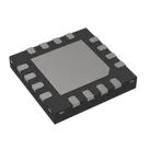
Yes — for MAX98357AETE+T, I’d group each pin exactly once like this:

Table


Functional groupPins
Power7 VDD, 8 VDD
Ground3 GND, 11 GND, 15 GND, EP Exposed Pad
Digital Audio Input / I²S-PCM1 DIN, 14 LRCLK, 16 BCLK
Configuration / Control2 GAIN_SLOT, 4 SD_MODE
Speaker Output9 OUTP, 10 OUTN
No Connect5 N.C., 6 N.C., 12 N.C., 13 N.C.
This keeps every datasheet pin in one group only; for Flux pin grouping, VDD-type pins belong under Power, GND/exposed pad under Ground, serial audio pins under Communication/Digital Audio, control/configuration pins under Control, OUTP/OUTN under Output, and N.C. pins under No Connect.
Fix pin groups
Set pin types
Check exposed pad
Run ERC check

To get started, talk to Flux or create a New Document.

Documents

    Documents are markdown text files which describe project goals, capture details, or even simulation outputs.

    Assets

    image-removebg-preview.png

    image-removebg-preview.png

    image-removebg-previewThumbnail
    kicad_mod

    QFN50P300X300X80-17N.kicad_mod

    FP_QFN50P300X300X80-17NFootprint
    stp

    MAX98357AETE+T.stp

    3D_MAX98357AETE+T3D Model

    MAX98357AETE+T

    MAX98357AETE+T thumbnail
    MAX98357A Series 5.5V 3.2W PCM Input Class D Audio Power Amplifier - TQFN-16
    The MAX98357A/MAX98357B is an easy-to-use, low-cost, digital pulse-code modulation (PCM) input Class D amplifier that provides industry-leading Class AB audio performance with Class D efficiency. The digital audio interface automatically recognizes up to 35 different PCM and TDM clocking schemes which eliminates the need for I2C programming. Operation is further simplified by eliminating the need for an external MCLK signal that is typically used for PCM communication. Simply supply power, LRCLK, BCLK, and digital audio to generate audio! Furthermore, a novel pinout allows customers to use the cost-effective WLP package with no need for expensive vias (refer to Application Note 6643: Optimize Cost, Size, and Performance with MAX98357 WLP for more information). The digital audio interface is highly flexible with the MAX98357A supporting I2S data and the MAX98357B supporting left-justified data. Both ICs support 8 channel time division multiplexed (TDM) data. The digital audio interface accepts specified sample rates between 8kHz and 96kHz for all supported data formats. The ICs can be configured to produce a left channel, right channel, or (left/2 + right/2) output from the stereo input data. The ICs operate using 16/24/32-bit data for I2S and left-justified modes as well as 16-bit or 32-bit data using TDM mode. The ICs eliminate the need for the external MCLK signal that is typically used for PCM communication. This reduces EMI and possible board coupling issues in addition to reducing the size and pin count of the ICs. The ICs also feature a very high wideband jitter tolerance (12ns typ) on BCLK and LRCLK to provide robust operation. Active emissions-limiting, edge-rate limiting, and overshoot control circuitry greatly reduce EMI. A filterless spread-spectrum modulation scheme eliminates the need for output filtering found in traditional Class D devices and reduces the component count of the solution. The ICs are available in 9-pin WLP (1.345mm x 1.435mm x 0.64mm) and 16-pin TQFN (3mm x 3mm x 0.75mm) packages and are specified over the -40°C to +85°C temperature range.
    ● Single-Supply Operation (2.5V to 5.5V) ● 3.2W Output Power into 4Ω at 5V ● 2.4mA Quiescent Current ● 92% Efficiency (RL = 8Ω, POUT = 1W) ● 22.8μVRMS Output Noise (AV = 15dB) ● Low 0.013% THD+N at 1kHz ● No MCLK Required ● Sample Rates of 8kHz to 96kHz ● Supports Left, Right, or (Left/2 + Right/2) Output ● Sophisticated Edge Rate Control Enables Filterless Class D Outputs ● 77dB PSRR at 1kHz ● Low RF Susceptibility Rejects TDMA Noise from GSM Radios ● Extensive Click-and-Pop Reduction Circuitry ● Robust Short-Circuit and Thermal Protection ● Available in Space-Saving Packages: 1.345mm x 1.435mm WLP (0.4mm Pitch) and 3mm x 3mm TQFN ● Solution Size with Single Bypass Capacitor is 4.32mm2 Applications ● Single Li-ion Cell/5V Devices ● Smart Speakers ● Notebook Computers ● IoT Devices ● Gaming Devices (Audio and Haptics) ● Smartphones ● Tablets ● Cameras

    Properties

    Integrated Circuit

    Analog Devices Inc./Maxim Integrated

    MAX98357AETE+T

    IC

    parametric-v1

    Pricing & Availability

    Distributor

    Qty 1

    Controls