Part Data Review and Validation
Thought for 5 mins 11 sec
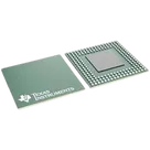
I reviewed the part project for IWR6843ARQGALP.
Step 1-2 status
Table
| Check | Result |
|---|---|
| MPN present | IWR6843ARQGALP |
| Description present | Single-chip 60-GHz to 64-GHz intelligent mmWave sensor with integrated antenna on package (AoP) |
| Datasheet URL present | Yes - Datasheet |
| Step 2 action required | No - Datasheet was already set, so no web lookup or property update was needed |
Table
| Field | Current project value | Datasheet / footprint evidence | Status |
|---|---|---|---|
| Part | IWR6843ARQGALP | TI mmWave AoP radar SoC | OK |
| Manufacturer | Texas Instruments | Texas Instruments | OK |
| Pin count | 180 | 180-pin package | OK |
| Package property | TO | FCCSP / FCBGA (ALP0180A), 15 mm x 15 mm, 0.8 mm pitch | Mismatch |
| Footprint asset | BGA180C80P18X18_1500X1500X96.kicad_mod | 18 x 18 grid, 15 mm body, 0.8 mm pitch, 0.96 mm height | Mostly aligned |
| Symbol pin mapping | 180 terminals with ball IDs | ALP0180A ball map rows A B C D E F G H J K L M N P R T U V, cols 1-18 | Looks aligned |
Table
| Category | Extracted data |
|---|---|
| Device description | AoP mmWave radar SoC with integrated 4 RX, 3 TX, PLL, ADC, baseband, DSP, hardware accelerator, and Arm Cortex-R4F subsystem |
| Frequency range | 60 GHz to 64 GHz |
| Bandwidth | 4 GHz continuous |
| TX beamforming | 6-bit phase shifter |
| Memory | 1.75 MB total with ECC |
| Interfaces | Up to 6 ADC channels, 2 SPI, 2 UART, 1 CAN-FD, I2C, GPIO, 2-lane LVDS |
| Clocking | 40.0 MHz crystal, external 40 MHz oscillator or driven clock |
| Operating junction temp | -40 C to 105 C |
| Package | 180-pin FCBGA/FCCSP, 15 mm x 15 mm, 0.8 mm pitch |
Table
| Parameter | Min | Max | Unit |
|---|---|---|---|
| VDDIN | -0.5 | 1.4 | V |
| VIN_SRAM | -0.5 | 1.4 | V |
| VNWA | -0.5 | 1.4 | V |
| VIOIN | -0.5 | 3.8 | V |
| VIOIN_18 | -0.5 | 2.0 | V |
| VIN_18CLK | -0.5 | 2.0 | V |
| VIOIN_18DIFF | -0.5 | 2.0 | V |
| VIN_13RF1 / VIN_13RF2 | -0.5 | 1.45 | V |
| VIN_13RF1 / VIN_13RF2 in 1 V LDO bypass mode | -0.5 | 1.4 | V |
| VIN_18BB | -0.5 | 2.0 | V |
| VIN_18VCO | -0.5 | 2.0 | V |
| Junction temperature | -40 | 105 | C |
| Storage temperature | -55 | 150 | C |
| Clamp current | -20 | 20 | mA |
Table
| Parameter | Min | Nom | Max | Unit |
|---|---|---|---|---|
| VDDIN | 1.14 | 1.2 | 1.32 | V |
| VIN_SRAM | 1.14 | 1.2 | 1.32 | V |
| VNWA | 1.14 | 1.2 | 1.32 | V |
| VIOIN 3.3 V mode | 3.13 | 3.3 | 3.45 | V |
| VIOIN 1.8 V mode | 1.71 | 1.8 | 1.89 | V |
| VIOIN_18 | 1.71 | 1.8 | 1.9 | V |
| VIN_18CLK | 1.71 | 1.8 | 1.9 | V |
| VIOIN_18DIFF | 1.71 | 1.8 | 1.9 | V |
| VIN_13RF1 / VIN_13RF2 | 1.23 | 1.3 | 1.36 | V |
| VIN_13RF1 / VIN_13RF2 bypass mode | 0.95 | 1.0 | 1.05 | V |
| VIN_18BB | 1.71 | 1.8 | 1.9 | V |
| VIN_18VCO | 1.71 | 1.8 | 1.9 | V |
Table
| Category | Value |
|---|---|
| Receiver effective isotropic noise figure | 9 dB |
| IF bandwidth | 10 MHz |
| ADC sampling rate, real/complex 2x | 25 Msps |
| ADC sampling rate, complex 1x | 12.5 Msps |
| ADC resolution | 12 bits |
| Idle channel spurs | -90 dBFS |
| Single-transmitter output power EIRP | 16 dBm |
| Power backoff range | 26 dB |
| Ramp rate | 250 MHz/us |
| Phase noise at 1 MHz offset | -93 dBc/Hz |
Table
| Category | Value |
|---|---|
| Max current on 1.2 V rails | 1000 mA |
| Max current on 1.3 V rails | 2000 mA |
| Peak current in 1 V bypass with 3 TX | 2500 mA |
| Max current on 1.8 V rails | 850 mA |
| Max current on 3.3 V rail | 50 mA |
| Typical average power, 24% duty, 1TX 4RX | 1.19 W |
| Typical average power, 24% duty, 2TX 4RX | 1.25 W |
| Typical average power, 48% duty, 1TX 4RX | 1.62 W |
| Typical average power, 48% duty, 2TX 4RX | 1.75 W |
| Theta JC | 2.6 C/W |
| Theta JB | 7.5 C/W |
| Theta JA | 20.3 C/W |
Table
| Group | Summary |
|---|---|
| Power rails | Separate rails for 1.2 V, 1.3 V, 1.8 V, LVDS, SRAM, VCO, and IO domains |
| Digital interfaces | SPIA/SPIB, QSPI, UART, CAN-FD, GPIO, JTAG, sync pins |
| Debug/data | DMM interface pins and LVDS outputs for raw ADC/debug |
| Pin muxing | Datasheet defines muxed functions and reset states by ball |
| Direction/type info | Datasheet includes per-ball I / O / IO typing and reset behavior |
Table
| Parameter | Datasheet value |
|---|---|
| Package code | ALP0180A |
| Package type | FCCSP / Plastic Ball Grid Array |
| Body size | 14.9 mm min to 15.1 mm max square |
| Height | 0.965 mm max |
| Ball pitch | 0.8 mm typ |
| Ball count | 180 |
| Ball diameter | 0.512 mm to 0.612 mm |
| Array span | 13.6 mm typ x 13.6 mm typ |
| Example board layout land size | 180 x 0.4 mm |
Table
| Check | Result | Risk |
|---|---|---|
| Pin count | 180 in symbol and 180 in footprint | Low |
| Ball naming/grid | Symbol terminals and footprint pads use datasheet-style ball IDs | Low |
| Package family | Footprint is clearly an 18 x 18, 0.8 mm pitch, 15 mm BGA | Low |
| Package property text | Project property says TO instead of ALP / FCCSP / FCBGA-180 | High for ordering/library metadata errors |
| Land size | Footprint pads appear to be 0.5 mm diameter, while datasheet example board layout shows 0.4 mm | High potential assembly / yield issue |
| Pin electrical types in symbol | Many symbol terminals are set to Unspecified instead of datasheet I/O types | Medium for ERC quality, lower for fabrication |
| Datasheet-to-footprint height/body | Footprint naming 1500X1500X96 matches 15 mm x 15 mm x 0.96 mm closely | Low |
Table
| Issue | Why it matters | Severity |
|---|---|---|
| Package or Case Code = TO | This does not match the actual package and could cause incorrect part ordering, bad library metadata, or confusion during reuse | Critical |
| Footprint pad diameter appears 0.5 mm vs datasheet example 0.4 mm land | This can affect solder joint geometry, paste definition, escape routing assumptions, and assembly yield | Critical |
| Symbol pin types are unspecified | Can weaken ERC and hide interface-direction mistakes | Moderate |
Table
| Area | Verdict |
|---|---|
| Datasheet availability | Good |
| Basic symbol pin count | Good |
| Ball-map alignment | Good |
| Footprint package size / pitch | Good |
| Metadata correctness | Needs correction |
| Land pattern confidence | Needs review before manufacturing |
The two items I would treat as blockers before releasing this part are:
- Correct the package metadata from TO to the proper ALP / FCCSP / FCBGA-180 package naming.
- Reconcile the footprint land diameter with the datasheet example board layout: current footprint shows 0.5 mm pads, datasheet example shows 0.4 mm.
If you want, I can next produce a pin-by-pin audit table for the symbol against the datasheet ball map.
Pin-by-pin audit
Check package metadata
Review land pattern
Library comparison


Welcome 👋
Flux accelerates your PCB design with AI.
Create your account to start using this component and bring your ideas to life.